| Tutorial Project: Exploring Digital Filters
|

|
|
Objective: In this project, you will build different types of lowpass and bandpass filters using virtual blocks.
|
|
Concepts/Features:
- Digital Filter
- Sampling Frequency
- Delay Element
- Z-Domain Transfer Function
- FIR Filter
- IIR Filter
- Signal Sampler
- Random Pulse Generator
|
|
Minimum Version Required: All versions
|
|
' Download Link: [1] Download Link: [1]
|
What You Will Learn
In this tutorial you will learn how to use RF.Spice's black-box virtual blocks to realize different types of filters with arbitrary transfer functions.
A Note on RF.Spice's Generic Digital Filter Block
In RF.Spice A/D the generic digital filter block is defined by its Z-domain transfer function, which is a rational function of the Z-transform variable:
[math] H(z) = \frac{N(z)}{D(z)} = \frac{ \sum_{m=0}^{M} b_m z^m }{ \sum_{n=0}^{N} a_n z^n } [/math]
with the assumption that N ≥ M.
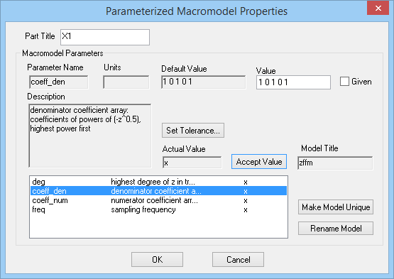
You need to specify the highest polynomial degree (N) and enter arrays of polynomial coefficients for the numerator and denominator of the transfer function in the property dialog of the generic digital filter block. This part can be accessed from Menu > Parts > Digital Signal Processing Blocks > Generic Digital Filter Block. To open the property dialog of this device, double-click on its symbol and then click the Edit Model... button.
 The property dialog of the Generic Digital Filter Block: the outer dialog. |
 The property dialog of the Generic Digital Filter Block: the inner dialog. |
 |
For a regular digital filter, you need to insert zero padding among the numerator and denominator polynomial coefficients.
|
For example, the coefficient array for a polynomial P(z) = z2 + z + 1 must be entered as "1 0 1 0 1". If the degree of the polynomial is N, then you need to enter a total of 2N+1 entries that include N padded zeros. The reason for this is RF.Spice A/D in fact constructs a polynomial in (-z1/2) behind the scene. So in reality, you enter the coefficients for the successive powers of (-z1/2):
[math] P(z) = z^2 + z + 1 = \sum_{n=0}^{N} a_n z^n = \sum_{k=0}^{2N} a^{\prime}_k (-z^{1/2})^k = 1(-z^{1/2})^4 + 0(-z^{1/2})^3 + 1(-z^{1/2})^2 + 0(-z^{1/2}) + 1 [/math]
Note that the term z-1/2 corresponds to a delay equal to half the sampling period.
Testing a Basic Delay Element
The following is a list of parts needed for this part of the tutorial lesson:
|
|
| Part Name
|
Part Type
|
Part Value
|
| V1
|
Finite Sequence Pulse Generator
|
Waveform TBD
|
| R1
|
Resistor
|
100
|
| X1
|
Generic Digital Filter Block
|
Defaults, deg = 1, Numer = "1", Denom = "1 0 0", freq = 1Hz
|
Place and connect the part as shown in the figure below:
 A simple circuit to test the generic digital filter block as a basic delay element. |
In the first part of this tutorial lesson, you will define a digital filter as a basic delay element. The Z-domain transfer function of this filter is given by:
[math]H(z) = z{-1/2} = \frac{1}{z} = \frac {0(-z^{1/2})^2 + 0(-z^{1/2}) + 1}{1(-z^{1/2})^2 + 0(-z^{1/2}) + 0} [/math]
This means that N= 1, M = 0, the coefficients of the denominator must be "1 0 0" and the numerator has only one coefficient "1". You don't have to enter the leading zero coefficients in the numerator.
As the source of your circuit, you are going to define five pulse of period 1s with a duty cycle of 20%. For this purpose, you can use a Finite Sequence Pulse Generator, which can be accessed from Parts > Waveform Generation Blocks > Basic Waveforms >.
Open the property dialog of the transfer function block. Change the denominator polynomial coefficients to "[1 1.4142 1]" and set the value of Denormalization Frequency to 6.283185Meg ( = 2π × 106 rad/s). In other words, you want a lowpass filter with a cutoff frequency of 1MHz.
 |
The denormalization frequency of the S-domain transfer function block must be expressed as an angular frequency in radians/second.
|
 The property dialog of the S-domain transfer function block. |
Run an AC frequency sweep of your filter with the following parameters:
|
|
| Start Frequency
|
1Hz
|
| Stop Frequency
|
100MHz
|
| Steps/Interval
|
50
|
| Interval Type
|
Decade
|
| Preset Graph Plots
|
Custom: Gain = VDB(2)
|
The frequency response is shown in the figure below as you should have expected:
 The frequency response of the second-order Butterworth loswpass filter. |
Building an FIR Filter: The Moving Average Filter
In this part of the tutorial lesson, create three more S-domain transfer function blocks and cascaded them as shown in the figure below. Copy and paste the additional parts since you want them to have the same properties as part A1.
 The schematic of the cascaded lowpass filter using transfer function virtual blocks. |
You will introduce four output voltages at Nodes 2, 3, 4 and 5. These correspond to second-order, fourth-order, sixth-order and eighth-order filter transfer functions, respectively. Note that the higher-order transfer functions realized in this way are different than the fourth-order, sixth-order and eighth-order Butterworth filter responses:
[math]H_{B4}(s) = \frac {1}{(s^2 + 0.7654s + 1)(s^2 + 1.8478s + 1)} \ne \left( \frac {1}{s^2 + 1.4142s + 1} \right)^2 [/math]
[math]H_{B6}(s) = \frac {1}{(s^2 + 0.5176s + 1)(s^2 + 1.4142s + 1)(s^2 + 1.9319s + 1)} \ne \left( \frac {1}{s^2 + 1.4142s + 1} \right)^3 [/math]
[math]H_{B8}(s) = \frac {1}{(s^2 + 0.3902s + 1)(s^2 + 1.1111s + 1)(s^2 + 1.6629s + 1)(s^2 + 1.9616s + 1)} \ne \left( \frac {1}{s^2 + 1.4142s + 1} \right)^4 [/math]
Run an AC frequency sweep of your cascaded filter with the parameters specified below:
|
|
| Start Frequency
|
1Hz
|
| Stop Frequency
|
1GHz
|
| Steps/Interval
|
50
|
| Interval Type
|
Decade
|
| Preset Graph Plots
|
Custom: Gain = VDB(2), VDB(3), VDB(4), VDB(5)
|
The results are shown in the figure below:
 The frequency response of the cascaded Butterworth loswpass filter. |
Testing Cascaded Chebyshev Lowpass Filters
The following is a list of parts needed for this part of the tutorial lesson:
|
|
| Part Name
|
Part Type
|
Part Value
|
| V1
|
Voltage Source
|
1V
|
| R1
|
Resistor
|
100
|
| A1 - A4
|
S-Domain Transfer Function Block
|
Defaults
|
The poles of the second-order Chebyshev filter of Type I are given by:
[math] s = \pm \frac{1}{\sqrt{2}} \sinh \left( \frac{1}{2} \sinh^{-1} \left( \frac{1}{\epsilon} \right) \right) + \frac{j}{\sqrt{2}} \cosh \left( \frac{1}{2} \sinh^{-1} \left( \frac{1}{\epsilon} \right) \right)[/math]
where ε is the ripple factor. The maximum passband ripple is given by:
[math] R_{dB} = 20\log \left( \frac{1}{1/\sqrt{1+\epsilon^2}} \right) [/math]
With a ripple factor ε = 1, the maximum peak-to-peak ripples would be 3dB, and the poles are given by:
[math] s = \pm 0.3218 +j 0.7769 [/math]
The transfer function of the second-order Chebyshev filter with ε = 1 is thus given by:
[math]H(s) = \frac {1} {1.4142s^2 + 0.911s + 1} [/math]
Use the circuit of the previous part. Open the property dialog of the transfer function block A1 and change the denominator coefficients to "[1.4142 0.911 1]". Note that XSPICE process devices share the same modes. As you change the properties of A1, the properties of all the other transfer function blocks A2, A3 and A4 are updated accordingly unless you make their models unique.
Run an AC frequency sweep of your new cascaded filter with the parameters specified below:
|
|
| Start Frequency
|
1Hz
|
| Stop Frequency
|
1GHz
|
| Steps/Interval
|
50
|
| Interval Type
|
Decade
|
| Preset Graph Plots
|
Custom: Gain = VDB(2), VDB(3), VDB(4), VDB(5)
|
The results are shown in the figure below:
 The frequency response of the cascaded Chebyshev loswpass filter. |
You can see the ripple in the passband of the filter. To better see the details, change the left axis limits to min = -10dB and max = 15dB with 5 divisions as shown in the figure below. Note that the maximum ripple of v(2) is 3dB as expected.
 A close-up of the passband region of the cascaded Chebyshev loswpass filter. |
Examining a Fourth-Order Chebyshev Filter
The following is a list of parts needed for this part of the tutorial lesson:
|
|
| Part Name
|
Part Type
|
Part Value
|
| V1
|
Voltage Source
|
1V
|
| R1
|
Resistor
|
100
|
| A1
|
S-Domain Transfer Function Block
|
Defaults
|
The transfer function of the fourth-order Chebyshev filter with ε = 1 is thus given by:
[math]H(s) = \frac {1} {5.65s^4 + 3.29s^3 + 6.60s^2 + 2.29s + 1} [/math]
Place and connect the part similar to the first part of this tutorial with a single block. In the property dialog of the transfer function block, set the denominator polynomial coefficients
to "[5.65s 3.29 6.60 2.29 1]" and set the value of Denormalization Frequency to 6.283185Meg.
Run an AC frequency sweep of your filter with the following parameters:
|
|
| Start Frequency
|
1Hz
|
| Stop Frequency
|
100MHz
|
| Steps/Interval
|
50
|
| Interval Type
|
Decade
|
| Preset Graph Plots
|
Custom: Gain = VDB(2)
|
The frequency response of the fourth-order Chebyshev filter is shown in the figure below, where you see several passband ripples. Compare this to the single ripple of the fourth-order filter in the previous section, which was made up two cascaded second-order Chebyshev filters.
 The frequency response of the fourth-order Chebyshev loswpass filter. |
Realizing a Second-Order Chebyshev Bandpass Filter
The following is a list of parts needed for this part of the tutorial lesson:
|
|
| Part Name
|
Part Type
|
Part Value
|
| V1
|
Voltage Source
|
1V
|
| R1
|
Resistor
|
100
|
| A1
|
S-Domain Transfer Function Block
|
Defaults
|
According to the filter theory, you can use the following transformation to realize a normalized bandpass filter from a normalized lowpass prototype:
[math] s \rightarrow \frac{1}{\Delta} \left( s + \frac{1}{s} \right) [/math]
where Δ = (ω2 - ω1)/ω0 is the fractional bandwidth. If you substitute the above transformation in the second-order Chebyshev s-domain transfer function, the following transfer function is obtained:
[math]H(s) = \frac {s^2} {22.627s^4 + 3.644s^3 + 46.254s^2 + 3.644s + 22.627} [/math]
Place and connect the parts similar to the first part of this tutorial with a single block. In the property dialog of the transfer function block, set the denominator polynomial coefficients
to "[22.627 3.644s 46.254 3.644 22.627]", set the numerator polynomial coefficients to "[1 0 0]", and set the value of Denormalization Frequency to 6.283185Meg.
Run an AC frequency sweep of your filter with the following parameters:
|
|
| Start Frequency
|
1k
|
| Stop Frequency
|
3MHz
|
| Steps/Interval
|
1k
|
| Interval Type
|
Linear
|
| Preset Graph Plots
|
Custom: Gain = VDB(2)
|
The frequency response of the second-order Chebyshev bandpass filter is shown in the figure below. Note that a linear frequency has been chosen as opposed to the previous graphs, which had the default logarithmic X-axis scale. As you can see from the graph, the center frequency of the filter is 1MHz and its bandwidth is about 280kHz.
 The frequency response of the fourth-order Chebyshev bandpass filter. |
 Back to RF.Spice A/D Tutorial Gateway
Last modified on 8 October 2015, at 18:49


