Difference between revisions of "EM.Libera"
(→Modeling Lumped Circuits) |
|||
| Line 1: | Line 1: | ||
EM.Libera is a 3D free-space structure simulator for modeling metallic structures. It features a full-wave Method of Moments (MoM) engine for analyzing wire structures or wire-frame models of metallic surfaces and solids. Many RF systems utilize wire antennas like dipoles, monopoles, loops, or arrays of wire antennas. The 3D method of moments (MoM) based on Pocklington's integral equation can accurately model such antennas and their coupling effects. Moreover, in many applications, metallic surface or [[Solid Objects|solid objects]] can be approximately modeled as wire-frame structures. EM.Libera's Wire MoM simulator can provide an adequate numerical solution of wire-frame structures. Examples of this sort are wire antennas in the presence of large reflectors or scatterers. Wire-frame models also make a good approximation of metallic target structures for radar cross section (RCS) analysis. | EM.Libera is a 3D free-space structure simulator for modeling metallic structures. It features a full-wave Method of Moments (MoM) engine for analyzing wire structures or wire-frame models of metallic surfaces and solids. Many RF systems utilize wire antennas like dipoles, monopoles, loops, or arrays of wire antennas. The 3D method of moments (MoM) based on Pocklington's integral equation can accurately model such antennas and their coupling effects. Moreover, in many applications, metallic surface or [[Solid Objects|solid objects]] can be approximately modeled as wire-frame structures. EM.Libera's Wire MoM simulator can provide an adequate numerical solution of wire-frame structures. Examples of this sort are wire antennas in the presence of large reflectors or scatterers. Wire-frame models also make a good approximation of metallic target structures for radar cross section (RCS) analysis. | ||
| − | EM.Libera's Wire MoM simulator is seamlessly interfaced with EM.CUBE's other simulation engines. The solution of a wire-frame structure can be imported to EM.Cube's other modules as a set of short dipole sources with proper amplitudes and phases. | + | EM.Libera's Wire MoM simulator is seamlessly interfaced with [[EM.Cube|EM.CUBE]]'s other simulation engines. The solution of a wire-frame structure can be imported to [[EM.Cube]]'s other modules as a set of short dipole sources with proper amplitudes and phases. |
== A 3D Method Of Moments Primer == | == A 3D Method Of Moments Primer == | ||
| Line 9: | Line 9: | ||
In a 3D MoM simulation, the currents or fields on the surface of a structure are the unknowns of the problem. The given structure is immersed in the free space. These currents or fields are discretized as a collection of elementary currents or fields with small finite spatial extents. Such elementary currents or fields are called basis functions. They obviously have a vectorial nature and must satisfy Maxwell's equations and relevant boundary conditions individually. The actual currents or fields on the surface of the given structure (the solution of the problem) are expressed as a superposition of these elementary currents or fields with initially unknown amplitudes. Through the MoM solution, you find these unknown amplitudes, from which you can then calculate the currents or fields everywhere in the structure. | In a 3D MoM simulation, the currents or fields on the surface of a structure are the unknowns of the problem. The given structure is immersed in the free space. These currents or fields are discretized as a collection of elementary currents or fields with small finite spatial extents. Such elementary currents or fields are called basis functions. They obviously have a vectorial nature and must satisfy Maxwell's equations and relevant boundary conditions individually. The actual currents or fields on the surface of the given structure (the solution of the problem) are expressed as a superposition of these elementary currents or fields with initially unknown amplitudes. Through the MoM solution, you find these unknown amplitudes, from which you can then calculate the currents or fields everywhere in the structure. | ||
| − | EM. | + | [[EM.Cube]]’s [[MoM3D Module|MoM3D module]] offers two distinct 3D MoM simulation engine. The first one is a Wire MoM solver that can be used to simulate wireframe models of metallic structures. This solver is particularly useful for modeling wire-type antennas and arrays. The second engine features a powerful surface MoM solver. It can model metallic surfaces and solids as well as solid dielectric objects. The Surface MoM solver uses a surface integral equation formulation of Maxwell's equations. In the case of solid dielectric objects, equivalent electric and magnetic currents are assumed on the surface of the dielectric object to formulate the interior and exterior boundary value problems. |
=== Free Space Green’s Function === | === Free Space Green’s Function === | ||
| Line 83: | Line 83: | ||
=== Galerkin Testing === | === Galerkin Testing === | ||
| − | The integral equation derived in the previous section can be solved numerically by discretizing the computational domain using a proper meshing scheme. The original functional equation is reduced to a set of discretized linear algebraic equations over elementary cells. The unknown quantities are found by solving this system of linear equations, and many other parameters can be computed thereafter. This method of numerical solution of integral equations is known as the Method of Moments (MoM). In this method, the unknown electric current is represented by an expansion of basis functions as follows: | + | The integral equation derived in the previous section can be solved numerically by discretizing the computational domain using a proper meshing scheme. The original functional equation is reduced to a set of discretized linear algebraic equations over elementary cells. The unknown quantities are found by solving this system of linear equations, and many other [[parameters]] can be computed thereafter. This method of numerical solution of integral equations is known as the Method of Moments (MoM). In this method, the unknown electric current is represented by an expansion of basis functions as follows: |
:<math> \mathbf{J(r)} = \sum_{n=1}^N {I_n}^{(J)} \mathbf{ {f_n}^{(J)}(r) }</math> | :<math> \mathbf{J(r)} = \sum_{n=1}^N {I_n}^{(J)} \mathbf{ {f_n}^{(J)}(r) }</math> | ||
| Line 154: | Line 154: | ||
=== Defining Groups Of PEC Objects === | === Defining Groups Of PEC Objects === | ||
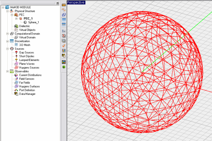
| − | EM.Cube's [[MoM3D Module]] features two different simulation engines: Wire MoM and Surface MoM. Both simulation engines can handle metallic structures. The Wire MoM engine models metallic objects as wireframe structures, while the Surface MoM engine treats them as perfect electric conductor (PEC) surfaces. The PEC objects can be lines, curves, surfaces or solids. All the PEC objects are created under the '''PEC''' node in the '''Physical Structure''' section of the Navigation Tree. Objects are grouped together by their color. You can insert different PEC groups with different colors. A new PEC group can be defined by simply right clicking on the '''PEC''' item in the Navigation Tree and selecting '''Insert New PEC...''' from the contextual menu. A dialog for setting up the PEC properties opens up. From this dialog you can change the name of the group or its color. Note that PEC object do not have any material properties that can be edited. | + | [[EM.Cube]]'s [[MoM3D Module]] features two different simulation engines: Wire MoM and Surface MoM. Both simulation engines can handle metallic structures. The Wire MoM engine models metallic objects as wireframe structures, while the Surface MoM engine treats them as perfect electric conductor (PEC) surfaces. The PEC objects can be lines, curves, surfaces or solids. All the PEC objects are created under the '''PEC''' node in the '''Physical Structure''' section of the Navigation Tree. Objects are grouped together by their color. You can insert different PEC groups with different colors. A new PEC group can be defined by simply right clicking on the '''PEC''' item in the Navigation Tree and selecting '''Insert New PEC...''' from the contextual menu. A dialog for setting up the PEC properties opens up. From this dialog you can change the name of the group or its color. Note that PEC object do not have any material properties that can be edited. |
[[File:wire_pic1.png]] [[File:wire_pic2.png]] | [[File:wire_pic1.png]] [[File:wire_pic2.png]] | ||
| Line 164: | Line 164: | ||
[[File:FDTD4.png|thumb|250px|[[MoM3D Module]]'s Dielectric dialog]] | [[File:FDTD4.png|thumb|250px|[[MoM3D Module]]'s Dielectric dialog]] | ||
| − | Of the two simulation engines of EM.Cube's [[MoM3D Module]] only the Surface MoM solver can handle dielectric objects as dielectric materials cannot be modeled by wireframe structures. Dielectric objects are created under the '''Dielectric''' node in the '''Physical Structure''' section of the Navigation Tree. They are grouped together by their color and material properties. You can insert different dielectric groups with different colors and different permittivity e<sub>r</sub> and electric conductivity s. Note that a PEC object is the limiting cases of a lossy dielectric material when σ → ∞. | + | Of the two simulation engines of [[EM.Cube]]'s [[MoM3D Module]] only the Surface MoM solver can handle dielectric objects as dielectric materials cannot be modeled by wireframe structures. Dielectric objects are created under the '''Dielectric''' node in the '''Physical Structure''' section of the Navigation Tree. They are grouped together by their color and material properties. You can insert different dielectric groups with different colors and different permittivity e<sub>r</sub> and electric conductivity s. Note that a PEC object is the limiting cases of a lossy dielectric material when σ → ∞. |
To define a new Dielectric group, follow these steps: | To define a new Dielectric group, follow these steps: | ||
| Line 170: | Line 170: | ||
* Right click on the '''Dielectric''' item of the Navigation Tree and select '''Insert New Dielectric...''' from the contextual menu. | * Right click on the '''Dielectric''' item of the Navigation Tree and select '''Insert New Dielectric...''' from the contextual menu. | ||
* Specify a '''Label''', '''Color''' (and optional Texture) and the electromagnetic properties of the dielectric material to be created: '''Relative Permittivity''' (e<sub>r</sub>) and '''Electric Conductivity''' (s). | * Specify a '''Label''', '''Color''' (and optional Texture) and the electromagnetic properties of the dielectric material to be created: '''Relative Permittivity''' (e<sub>r</sub>) and '''Electric Conductivity''' (s). | ||
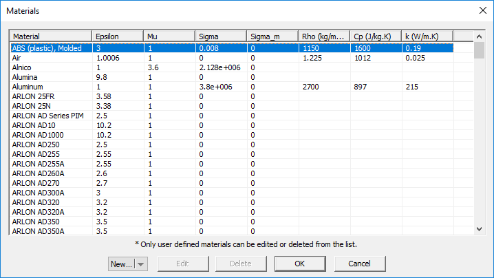
| − | * You may also choose from a list of preloaded material types. Click the button labeled '''Material''' to open EM.Cube's Materials dialog. Select the desired material from the list or type the first letter of a material to find it. For example, typing '''V''' selects '''Vacuum''' in the list. Once you close the dialog by clicking '''OK''', the selected material properties fill the parameter fields automatically. | + | * You may also choose from a list of preloaded material types. Click the button labeled '''Material''' to open [[EM.Cube]]'s Materials dialog. Select the desired material from the list or type the first letter of a material to find it. For example, typing '''V''' selects '''Vacuum''' in the list. Once you close the dialog by clicking '''OK''', the selected material properties fill the parameter fields automatically. |
* Click the '''OK''' button of the dielectric material dialog to accept the changes and close it. | * Click the '''OK''' button of the dielectric material dialog to accept the changes and close it. | ||
[[File:FDTD5.png]] | [[File:FDTD5.png]] | ||
| − | Figure: EM.Cube's material list. | + | Figure: [[EM.Cube]]'s material list. |
=== Moving Objects Between Groups & Modules === | === Moving Objects Between Groups & Modules === | ||
| − | By default, the last PEC group that was defined is active. The current active group is always listed in bold letters in the Navigation Tree. All the new objects are inserted under the current active group. A group can be activated with a right click on its entry in the Navigation Tree and then selecting the '''Active''' item of the contextual menu. You can move one or more selected objects to any desired PEC group. Right click on the highlighted selection and select '''Move To [[File:larrow_tn.png]] MoM3D [[File:larrow_tn.png]]''' from the contextual menu. This opens another sub-menu with a list of all the available PEC groups already defined in the [[PO Module]]. Select the desired PEC group, and all the selected objects will move to that group. The objects can be selected either in the project workspace, or their names can be selected from the Navigation Tree. In the latter case, make sure that you hold the keyboard's '''Shift Key''' or '''Ctrl Key''' down while selecting a PEC group's name from the contextual menu. In a similar way, you can move one or more objects from a Physical Optics PEC group to EM.CUBE's other modules. In this case, the sub-menus of the''' Move To [[File:larrow_tn.png]]''' item of the contextual menu will indicate all the EM.CUBE modules that have valid groups for transfer of the select objects. | + | By default, the last PEC group that was defined is active. The current active group is always listed in bold letters in the Navigation Tree. All the new objects are inserted under the current active group. A group can be activated with a right click on its entry in the Navigation Tree and then selecting the '''Active''' item of the contextual menu. You can move one or more selected objects to any desired PEC group. Right click on the highlighted selection and select '''Move To [[File:larrow_tn.png]] MoM3D [[File:larrow_tn.png]]''' from the contextual menu. This opens another sub-menu with a list of all the available PEC groups already defined in the [[PO Module]]. Select the desired PEC group, and all the selected objects will move to that group. The objects can be selected either in the project workspace, or their names can be selected from the Navigation Tree. In the latter case, make sure that you hold the keyboard's '''Shift Key''' or '''Ctrl Key''' down while selecting a PEC group's name from the contextual menu. In a similar way, you can move one or more objects from a Physical Optics PEC group to [[EM.Cube|EM.CUBE]]'s other modules. In this case, the sub-[[menus]] of the''' Move To [[File:larrow_tn.png]]''' item of the contextual menu will indicate all the [[EM.Cube|EM.CUBE]] modules that have valid groups for transfer of the select objects. |
=== 3D MoM Mesh Types === | === 3D MoM Mesh Types === | ||
| Line 187: | Line 187: | ||
=== Creating & Viewing The Mesh === | === Creating & Viewing The Mesh === | ||
| − | The [[MoM3D Module]]'s method of moments solver assumes an infinite open boundary for your project's structure and uses the free space Green's functions for the background structure. As a result, the extents of the computational domain are infinite in all directions. The mesh generation process in EM.CUBE's [[MoM3D Module]] involves three steps: | + | The [[MoM3D Module]]'s method of moments solver assumes an infinite open boundary for your project's structure and uses the free space Green's functions for the background structure. As a result, the extents of the computational domain are infinite in all directions. The mesh generation process in [[EM.Cube|EM.CUBE]]'s [[MoM3D Module]] involves three steps: |
# Setting the mesh properties. | # Setting the mesh properties. | ||
| Line 193: | Line 193: | ||
# Verifying the mesh. | # Verifying the mesh. | ||
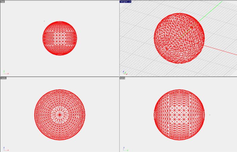
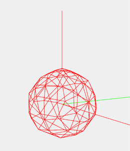
| − | The commercial release of EM.CUBE's [[MoM3D Module]] provides a Wire MoM solver. In this simulation engine, all the metallic objects are discretized as a wire-frame structure. Wires, line and curves are discretized as polylines made up of small linear cells (segments).Surface and [[Solid Objects|solid objects]] are discretized as a wire-frame mesh with triangular cells. The MoM3D mesh generator meshes the wires based on a specified mesh sampling rate expressed in cells/&lambda<sub>0</sub>. Curves are first polygonized and converted into '''Polyline''' Objects, whose edge lengths follow the specified mesh sampling rate. In the case of [[Solid Objects|solid objects]], only their surface and faces are discretized using a triangular wireframe mesh, which is regarded as a grid of interconnected wires. Two algorithms are offered for generation of a triangular wireframe mesh. The default algorithm is '''Regular Wireframe'''. This mesh generator creates wireframe elements that have almost equal edge lengths. The other algorithm is '''Structured Wireframe''', which usually creates a very structured wireframe with a large number of aligned wireframe elements. | + | The commercial release of [[EM.Cube|EM.CUBE]]'s [[MoM3D Module]] provides a Wire MoM solver. In this simulation engine, all the metallic objects are discretized as a wire-frame structure. Wires, line and curves are discretized as polylines made up of small linear cells (segments).Surface and [[Solid Objects|solid objects]] are discretized as a wire-frame mesh with triangular cells. The MoM3D mesh generator meshes the wires based on a specified mesh sampling rate expressed in cells/&lambda<sub>0</sub>. Curves are first polygonized and converted into '''Polyline''' Objects, whose edge lengths follow the specified mesh sampling rate. In the case of [[Solid Objects|solid objects]], only their surface and faces are discretized using a triangular wireframe mesh, which is regarded as a grid of interconnected wires. Two algorithms are offered for generation of a triangular wireframe mesh. The default algorithm is '''Regular Wireframe'''. This mesh generator creates wireframe elements that have almost equal edge lengths. The other algorithm is '''Structured Wireframe''', which usually creates a very structured wireframe with a large number of aligned wireframe elements. |
| − | To view the [[MoM3D Module]]'s wire-frame mesh, click on the [[File:mesh_tool_tn.png]] button of the '''Compute Toolbar''' or select '''Menu [[File:larrow_tn.png]] Compute [[File:larrow_tn.png]] Discretization [[File:larrow_tn.png]] Shoe Mesh''' or use the keyboard shortcut '''Ctrl+M'''. When the wire-frame mesh is displayed in the Project Workspace, EM.CUBE's mesh view mode is enabled. In this mode, you can perform view operations like rotate view, pan, zoom, etc. However, you cannot select or move or edit objects. While the mesh view is enabled, the '''Show Mesh''' [[File:mesh_tool.png]] button remains depressed. To get back to the Normal View mode, click this button one more time, or deselect '''Menu [[File:larrow_tn.png]] Compute [[File:larrow_tn.png]] Discretization [[File:larrow_tn.png]] Show Mesh''' to remove its check mark or simply click the '''Esc Key''' of the keyboard."Show Mesh" generates a new mesh and displays it if there is none in the memory, or it simply displays an existing mesh in the memory. This is a useful feature because generating a wire-frame mesh may take a long time depending on the complexity and size of objects. If you change the structure or alter the mesh settings, a new mesh is always generated. You can ignore the mesh in the memory and force EM.CUBE to generate a mesh from the ground up by selecting '''Menu [[File:larrow_tn.png]] Compute [[File:larrow_tn.png]] Discretization [[File:larrow_tn.png]] Regenerate Mesh''' or by right clicking on the '''3-D Mesh''' item of the Navigation Tree and selecting '''Regenerate''' from the contextual menu. | + | To view the [[MoM3D Module]]'s wire-frame mesh, click on the [[File:mesh_tool_tn.png]] button of the '''Compute Toolbar''' or select '''Menu [[File:larrow_tn.png]] Compute [[File:larrow_tn.png]] Discretization [[File:larrow_tn.png]] Shoe Mesh''' or use the keyboard shortcut '''Ctrl+M'''. When the wire-frame mesh is displayed in the Project Workspace, [[EM.Cube|EM.CUBE]]'s mesh view mode is enabled. In this mode, you can perform view operations like rotate view, pan, zoom, etc. However, you cannot select or move or edit objects. While the mesh view is enabled, the '''Show Mesh''' [[File:mesh_tool.png]] button remains depressed. To get back to the Normal View mode, click this button one more time, or deselect '''Menu [[File:larrow_tn.png]] Compute [[File:larrow_tn.png]] Discretization [[File:larrow_tn.png]] Show Mesh''' to remove its check mark or simply click the '''Esc Key''' of the keyboard."Show Mesh" generates a new mesh and displays it if there is none in the memory, or it simply displays an existing mesh in the memory. This is a useful feature because generating a wire-frame mesh may take a long time depending on the complexity and size of objects. If you change the structure or alter the mesh settings, a new mesh is always generated. You can ignore the mesh in the memory and force [[EM.Cube|EM.CUBE]] to generate a mesh from the ground up by selecting '''Menu [[File:larrow_tn.png]] Compute [[File:larrow_tn.png]] Discretization [[File:larrow_tn.png]] Regenerate Mesh''' or by right clicking on the '''3-D Mesh''' item of the Navigation Tree and selecting '''Regenerate''' from the contextual menu. |
[[File:wire_pic5_tn.png]] | [[File:wire_pic5_tn.png]] | ||
| Line 213: | Line 213: | ||
=== Mesh of Connected Objects === | === Mesh of Connected Objects === | ||
| − | All the [[Solid Objects|solid objects]] belonging to the same PEC group are merged together using the Boolean union operation before meshing. If your structure contains attached, interconnected or overlapping [[Solid Objects|solid objects]], their internal common faces are removed and only the surface of the external faces is meshed. Similarly, all the [[Surface Objects|surface objects]] belonging to the same PEC group are merged together before meshing. However, following EM.CUBE's union rules, a solid and a surface object cannot not be "unioned" together. Therefore, their meshes will not connect even if the two objects belong to the same PEC group. | + | All the [[Solid Objects|solid objects]] belonging to the same PEC group are merged together using the Boolean union operation before meshing. If your structure contains attached, interconnected or overlapping [[Solid Objects|solid objects]], their internal common faces are removed and only the surface of the external faces is meshed. Similarly, all the [[Surface Objects|surface objects]] belonging to the same PEC group are merged together before meshing. However, following [[EM.Cube|EM.CUBE]]'s union rules, a solid and a surface object cannot not be "unioned" together. Therefore, their meshes will not connect even if the two objects belong to the same PEC group. |
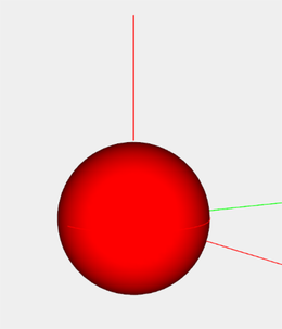
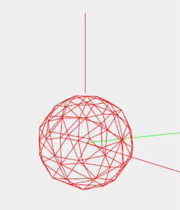
| − | You can connect a line object to a touching surface. To connect lines to surfaces and allow for current continuity, you must make sure that the box labeled '''Connect Lines to Touching Surfaces''' is checked in the '''Mesh Settings Dialog'''. If the end of a line lies on a flat surface, EM.CUBE will detect that and create the connection automatically. However, this may not always be the case if the surface is not flat and has curvature. In such cases, you have to specifically instruct EM.CUBE to enforce the connection. An example of this case is shown in the figure below. | + | You can connect a line object to a touching surface. To connect lines to surfaces and allow for current continuity, you must make sure that the box labeled '''Connect Lines to Touching Surfaces''' is checked in the '''Mesh Settings Dialog'''. If the end of a line lies on a flat surface, [[EM.Cube|EM.CUBE]] will detect that and create the connection automatically. However, this may not always be the case if the surface is not flat and has curvature. In such cases, you have to specifically instruct [[EM.Cube|EM.CUBE]] to enforce the connection. An example of this case is shown in the figure below. |
[[File:wire_pic7_tn.png|260px]] [[File:wire_pic8_tn.png|260px]] [[File:wire_pic9_tn.png|260px]] | [[File:wire_pic7_tn.png|260px]] [[File:wire_pic8_tn.png|260px]] [[File:wire_pic9_tn.png|260px]] | ||
| Line 223: | Line 223: | ||
=== Local Mesh Control === | === Local Mesh Control === | ||
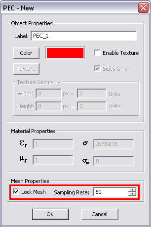
| − | EM.CUBE applies the global mesh sampling rate to discretize all the objects in the Project Workspace. However, you can lock the mesh sampling rate of any PEC group to a desired value different than the global rate. To do so, open the property dialog of a PEC group by right clicking on its name in the Navigation Tree and select '''Properties...''' from the contextual menu. At the bottom of the dialog, check the box labeled '''Lock Mesh'''. This will enable the '''Sampling Rate''' box, where you can set a desired value. The default value is equal to the global mesh sampling rate. Keep in mind that objects that belong to different PEC groups are not merged during the mesh generation even if they overlap or are intended to be connected to one another.<br /> | + | [[EM.Cube|EM.CUBE]] applies the global mesh sampling rate to discretize all the objects in the Project Workspace. However, you can lock the mesh sampling rate of any PEC group to a desired value different than the global rate. To do so, open the property dialog of a PEC group by right clicking on its name in the Navigation Tree and select '''Properties...''' from the contextual menu. At the bottom of the dialog, check the box labeled '''Lock Mesh'''. This will enable the '''Sampling Rate''' box, where you can set a desired value. The default value is equal to the global mesh sampling rate. Keep in mind that objects that belong to different PEC groups are not merged during the mesh generation even if they overlap or are intended to be connected to one another.<br /> |
[[File:wire_pic10.png]] | [[File:wire_pic10.png]] | ||
| Line 233: | Line 233: | ||
=== Gaps Sources On Wires === | === Gaps Sources On Wires === | ||
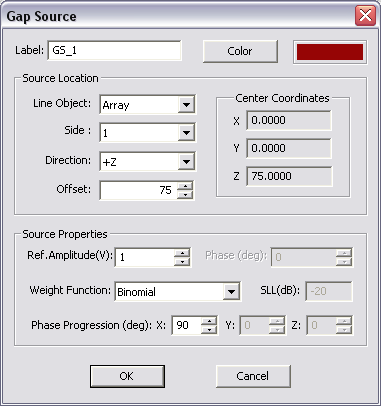
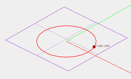
| − | A Gap is an infinitesimally narrow discontinuity that is placed on the path of the current. In EM.Cube's [[MoM3D Module]], a gap is used to define an excitation source in the form of an ideal voltage source. Gap sources can be placed only on '''Line''' and '''Polyline''' objects. '''If you want to excite a curved wire antennas such as a circular loop or helix with a gap source, first you have to convert the curve object into a polyline using EM.Cube's Polygonize Tool.''' The gap splits the wire into two segment with a an infinitesimally small spacing between them, across which the ideal voltage source is connected. To define a new gap source, follow these steps: | + | A Gap is an infinitesimally narrow discontinuity that is placed on the path of the current. In [[EM.Cube]]'s [[MoM3D Module]], a gap is used to define an excitation source in the form of an ideal voltage source. Gap sources can be placed only on '''Line''' and '''Polyline''' objects. '''If you want to excite a curved wire antennas such as a circular loop or helix with a gap source, first you have to convert the curve object into a polyline using [[EM.Cube]]'s Polygonize Tool.''' The gap splits the wire into two segment with a an infinitesimally small spacing between them, across which the ideal voltage source is connected. To define a new gap source, follow these steps: |
* Right click on the '''Gap Sources''' item in the '''Sources''' section of the Navigation Tree and select '''Insert New Source...''' from the contextual menu. The Gap Source Dialog opens up. | * Right click on the '''Gap Sources''' item in the '''Sources''' section of the Navigation Tree and select '''Insert New Source...''' from the contextual menu. The Gap Source Dialog opens up. | ||
| Line 250: | Line 250: | ||
[[File:wire_pic15.png|thumb|300px|[[MoM3D Module]]'s lumped element dialog]] | [[File:wire_pic15.png|thumb|300px|[[MoM3D Module]]'s lumped element dialog]] | ||
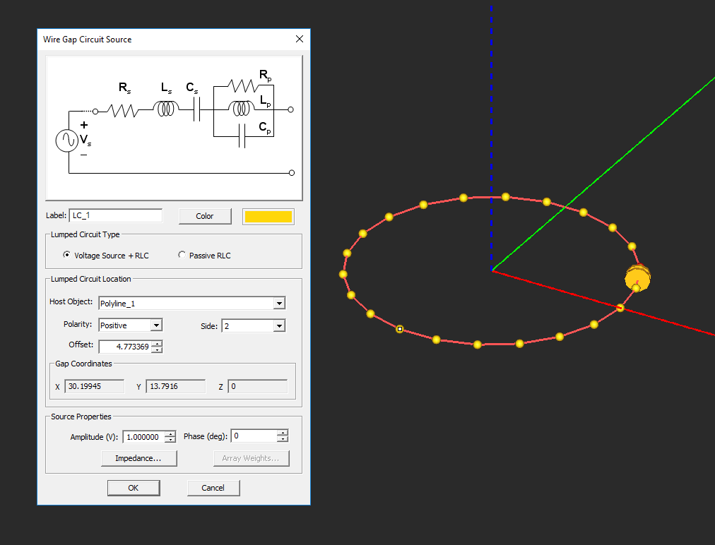
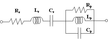
| − | In EM.Cube's [[MoM3D Module]], you can define simple lumped elements in a similar manner as gap sources. In fact, a lumped element is equivalent to an infinitesimally narrow gap that is placed in the path of the current, across which Ohm's law is enforced as a boundary condition. You can define passive RLC lumped elements or active lumped elements containing a voltage gap source. The latter case can be used to excite a wire structure and model a non-ideal voltage source with an internal resistance. Unlike the [[FDTD Module]]'s single-device lumped loads that connect between two adjacent nodes, the [[MoM3D Module]]'s lumped circuit represent a series-parallel combination of resistor, inductor and capacitor elements. This is shown in the figure below: | + | In [[EM.Cube]]'s [[MoM3D Module]], you can define simple lumped elements in a similar manner as gap sources. In fact, a lumped element is equivalent to an infinitesimally narrow gap that is placed in the path of the current, across which Ohm's law is enforced as a boundary condition. You can define passive RLC lumped elements or active lumped elements containing a voltage gap source. The latter case can be used to excite a wire structure and model a non-ideal voltage source with an internal resistance. Unlike the [[FDTD Module]]'s single-device lumped loads that connect between two adjacent nodes, the [[MoM3D Module]]'s lumped circuit represent a series-parallel combination of resistor, inductor and capacitor elements. This is shown in the figure below: |
[[File:image106.png]] | [[File:image106.png]] | ||
| Line 272: | Line 272: | ||
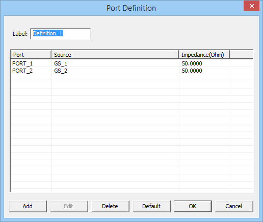
Ports are used to order and index gap sources for S parameter calculation. They are defined in the '''Observables''' section of the Navigation Tree. Right click on the '''Port Definition''' item of the Navigation Tree and select '''Insert New Port Definition...''' from the contextual menu. The Port Definition Dialog opens up, showing the total number of existing sources in the workspace. By default, as many ports as the total number of sources are created. You can define any number of ports equal to or less than the total number of sources. This includes both gap sources and active lumped elements (which contain gap sources). In the '''Port Association''' section of this dialog, you can go over each one of the sources and associate them with a desired port. Note that you can associate more than one source with same given port. In this case, you will have a coupled port. All the coupled sources are listed as associated with a single port. However, you cannot associate the same source with more than one port. Finally, you can assign '''Port Impedance''' in Ohms. By default, all port impedances are 50Σ. The table titled '''Port Configuration''' lists all the ports and their associated sources and port impedances. | Ports are used to order and index gap sources for S parameter calculation. They are defined in the '''Observables''' section of the Navigation Tree. Right click on the '''Port Definition''' item of the Navigation Tree and select '''Insert New Port Definition...''' from the contextual menu. The Port Definition Dialog opens up, showing the total number of existing sources in the workspace. By default, as many ports as the total number of sources are created. You can define any number of ports equal to or less than the total number of sources. This includes both gap sources and active lumped elements (which contain gap sources). In the '''Port Association''' section of this dialog, you can go over each one of the sources and associate them with a desired port. Note that you can associate more than one source with same given port. In this case, you will have a coupled port. All the coupled sources are listed as associated with a single port. However, you cannot associate the same source with more than one port. Finally, you can assign '''Port Impedance''' in Ohms. By default, all port impedances are 50Σ. The table titled '''Port Configuration''' lists all the ports and their associated sources and port impedances. | ||
| − | {{Note|In EM.CUBE you cannot assign ports to an array object, even if it contains sources on its elements. To calculate the S parameters of an antenna array, you have to construct it using individual elements, not as an array object.}} | + | {{Note|In [[EM.Cube|EM.CUBE]] you cannot assign ports to an array object, even if it contains sources on its elements. To calculate the S [[parameters]] of an antenna array, you have to construct it using individual elements, not as an array object.}} |
[[File:port-definition.png]] | [[File:port-definition.png]] | ||
| Line 297: | Line 297: | ||
* In the '''Direction Unit Vector''' section, you can specify the orientation of the short dipole by setting values for the components '''uX''', '''uY''', and '''uZ''' of the dipole's unit vector. The default values correspond to a vertical (Z-directed) short dipole. The dialog normalizes the vector components upon closure even if your component values do not satisfy a unit magnitude. | * In the '''Direction Unit Vector''' section, you can specify the orientation of the short dipole by setting values for the components '''uX''', '''uY''', and '''uZ''' of the dipole's unit vector. The default values correspond to a vertical (Z-directed) short dipole. The dialog normalizes the vector components upon closure even if your component values do not satisfy a unit magnitude. | ||
| − | When you simulate a wire structure in the [[MoM3D Module]], you can define a '''Current Distribution Observable''' in your project. This is used not only to visualize the current distribution in the project workspace but also to save the current solution into an ASCII data file. This data file is called "MoM.IDI" by default and has a '''.IDI''' file extension. The current data are saved as line segments representing each of the wire cells together with the complex current at the center of each cell. In the [[MoM3D Module]], you can import the current data from an existing '''.IDI''' file to serve as a set of short dipoles for excitation. To import a wire current solution, right click on '''Short Dipoles''' item in the '''Sources''' section of the Navigation Tree and select '''Import Dipole Source...''' from the contextual menu. This opens up the standard Windows Open dialog with the file type set to '''.IDI'''. Browse your folders to find the right current data file. Once you find it, select it and click the '''Open''' button of the dialog. This will create as many short dipole sources on the [[PO Module]]'s Navigation Tree as the total number of mesh cells in the Wire MoM solution. From this point on, each of the imported dipoles behave like a regular short dipole source. You can open the property dialog of each individual source and modify its parameters. | + | When you simulate a wire structure in the [[MoM3D Module]], you can define a '''Current Distribution Observable''' in your project. This is used not only to visualize the current distribution in the project workspace but also to save the current solution into an ASCII data file. This data file is called "MoM.IDI" by default and has a '''.IDI''' file extension. The current data are saved as line segments representing each of the wire cells together with the complex current at the center of each cell. In the [[MoM3D Module]], you can import the current data from an existing '''.IDI''' file to serve as a set of short dipoles for excitation. To import a wire current solution, right click on '''Short Dipoles''' item in the '''Sources''' section of the Navigation Tree and select '''Import Dipole Source...''' from the contextual menu. This opens up the standard [[Windows]] Open dialog with the file type set to '''.IDI'''. Browse your folders to find the right current data file. Once you find it, select it and click the '''Open''' button of the dialog. This will create as many short dipole sources on the [[PO Module]]'s Navigation Tree as the total number of mesh cells in the Wire MoM solution. From this point on, each of the imported dipoles behave like a regular short dipole source. You can open the property dialog of each individual source and modify its [[parameters]]. |
=== Plane Wave Sources === | === Plane Wave Sources === | ||
| Line 303: | Line 303: | ||
[[File:po_phys15.png|thumb|300px|plane wave dialog]] | [[File:po_phys15.png|thumb|300px|plane wave dialog]] | ||
| − | The wire-frame structure in the [[MoM3D Module]] can be excited by an incident plane wave. In particular, a plane wave source can be used to compute the radar cross section of a metallic target. A plane wave is defined by its propagation vector indicating the direction of incidence and its polarization. EM.CUBE's [[MoM3D Module]] provides the following polarization options: | + | The wire-frame structure in the [[MoM3D Module]] can be excited by an incident plane wave. In particular, a plane wave source can be used to compute the radar cross section of a metallic target. A plane wave is defined by its propagation vector indicating the direction of incidence and its polarization. [[EM.Cube|EM.CUBE]]'s [[MoM3D Module]] provides the following polarization options: |
* TMz | * TMz | ||
| Line 331: | Line 331: | ||
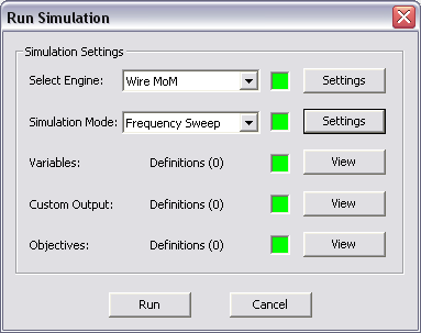
[[File:wire_pic19.png|thumb|300px|[[MoM3D Module]]'s run simulation dialog]] | [[File:wire_pic19.png|thumb|300px|[[MoM3D Module]]'s run simulation dialog]] | ||
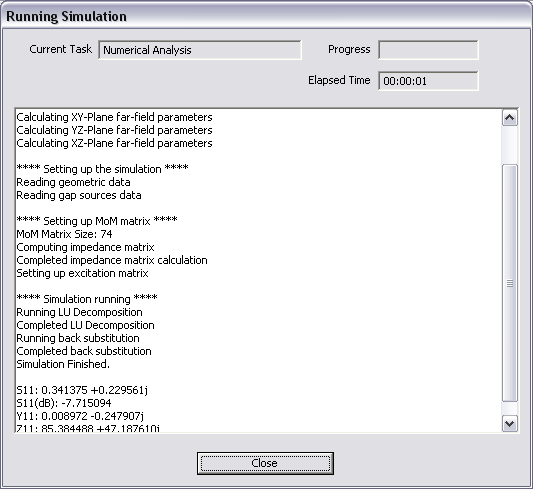
| − | Once you have set up your metal structure in EM.CUBE's [[MoM3D Module]], have defined sources and observables and have examined the quality of the structure's wire-frame mesh, you are ready to run a simulation. To open the Run Simulation Dialog, click the '''Run''' [[File:run_icon.png]] button of the '''Compute Toolbar''' or select Menu [[File:larrow_tn.png]] Compute [[File:larrow_tn.png]] Run...or use the keyboard shortcut '''Ctrl+R'''. To start the simulation click the '''Run''' button of this dialog. Once the Wire MoM simulation starts, a new dialog called '''Output Window''' opens up that reports the various stages of Wire MoM simulation, displays the running time and shows the percentage of completion for certain tasks during the Wire MoM simulation process. A prompt announces the completion of the Wire MoM simulation. At this time, EM.CUBE generates a number of output data files that contain all the computed simulation data. These include current distributions, near field data, far field radiation pattern data as well bi-static or mono-static radar cross sections (RCS) if the structure is excited by a plane wave source. | + | Once you have set up your metal structure in [[EM.Cube|EM.CUBE]]'s [[MoM3D Module]], have defined sources and observables and have examined the quality of the structure's wire-frame mesh, you are ready to run a simulation. To open the Run Simulation Dialog, click the '''Run''' [[File:run_icon.png]] button of the '''Compute Toolbar''' or select Menu [[File:larrow_tn.png]] Compute [[File:larrow_tn.png]] Run...or use the keyboard shortcut '''Ctrl+R'''. To start the simulation click the '''Run''' button of this dialog. Once the Wire MoM simulation starts, a new dialog called '''Output Window''' opens up that reports the various stages of Wire MoM simulation, displays the running time and shows the percentage of completion for certain tasks during the Wire MoM simulation process. A prompt announces the completion of the Wire MoM simulation. At this time, [[EM.Cube|EM.CUBE]] generates a number of output data files that contain all the computed simulation data. These include current distributions, near field data, far field radiation pattern data as well bi-static or mono-static radar cross sections (RCS) if the structure is excited by a plane wave source. |
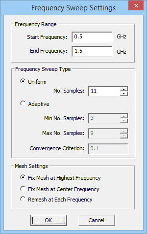
You have the choice to run a '''Fixed Frequency''' simulation, which is the default choice, or run a '''Frequency Sweep'''. In the former case, the simulation will be carried out at the '''Center Frequency''' of the project. This frequency can be changed from the Frequency Dialog of the project or you can click the Frequency Settings button of the Run Dialog to open up the Frequency Settings dialog. You can change the value of Center Frequency from this dialog, too. | You have the choice to run a '''Fixed Frequency''' simulation, which is the default choice, or run a '''Frequency Sweep'''. In the former case, the simulation will be carried out at the '''Center Frequency''' of the project. This frequency can be changed from the Frequency Dialog of the project or you can click the Frequency Settings button of the Run Dialog to open up the Frequency Settings dialog. You can change the value of Center Frequency from this dialog, too. | ||
| Line 343: | Line 343: | ||
=== Setting Wire MoM Numerical Parameters === | === Setting Wire MoM Numerical Parameters === | ||
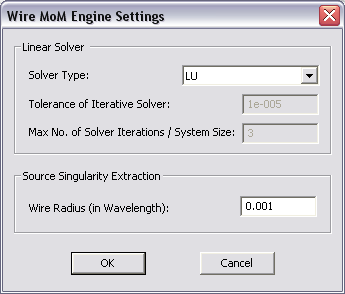
| − | A Wire MoM simulation involves a number of numerical parameters that normally take default values unless you change them. You can access these parameters and change their values by clicking on the '''Settings''' button next to the "Select Engine" drop-down list in the '''Run Dialog'''. This opens up the Wire MoM Engine Settings Dialog. In the '''Solver''' section of the dialog, you can choose the type of linear solver. The current options are '''LU''' and '''Bi-Conjugate Gradient (BiCG)'''. The LU solver is a direct solver and is the default option of the [[MoM3D Module]]. The BiCG solver is iterative. Once selected, you have to set a '''Tolerance''' for its convergence. You can also change the maximum number of BiCG iterations by setting a new value for '''Max. No. of Solver Iterations / System Size'''. The Wire MoM simulator is based on Pocklington's integral equation method. In this method, the wires are assumed to have a very small radius. The basis functions are placed on the axis of the "wire cylinder", while the Galerkin testing is carried out on its surface to avoid the singularity of the Green's functions. In the "Source Singularity" section of the dialog, you can specify the '''Wire Radius''' . EM.CUBE's [[MoM3D Module]] assumes an identical wire radius for all wires and wireframe structures. This radius is expressed in free space wavelengths and its default value is 0.001λ<sub>0</sub>. The value of the wire radius has a direct influence on the wire's computed reactance. | + | A Wire MoM simulation involves a number of numerical [[parameters]] that normally take default values unless you change them. You can access these [[parameters]] and change their values by clicking on the '''Settings''' button next to the "Select Engine" drop-down list in the '''Run Dialog'''. This opens up the Wire MoM Engine Settings Dialog. In the '''Solver''' section of the dialog, you can choose the type of linear solver. The current options are '''LU''' and '''Bi-Conjugate Gradient (BiCG)'''. The LU solver is a direct solver and is the default option of the [[MoM3D Module]]. The BiCG solver is iterative. Once selected, you have to set a '''Tolerance''' for its convergence. You can also change the maximum number of BiCG iterations by setting a new value for '''Max. No. of Solver Iterations / System Size'''. The Wire MoM simulator is based on Pocklington's integral equation method. In this method, the wires are assumed to have a very small radius. The basis functions are placed on the axis of the "wire cylinder", while the Galerkin testing is carried out on its surface to avoid the singularity of the Green's functions. In the "Source Singularity" section of the dialog, you can specify the '''Wire Radius''' . [[EM.Cube|EM.CUBE]]'s [[MoM3D Module]] assumes an identical wire radius for all wires and wireframe structures. This radius is expressed in free space wavelengths and its default value is 0.001λ<sub>0</sub>. The value of the wire radius has a direct influence on the wire's computed reactance. |
[[File:wire_pic21.png]] | [[File:wire_pic21.png]] | ||
| Line 353: | Line 353: | ||
[[File:wire_pic25.png|thumb|300px|[[MoM3D Module]]'s current distribution dialog]] | [[File:wire_pic25.png|thumb|300px|[[MoM3D Module]]'s current distribution dialog]] | ||
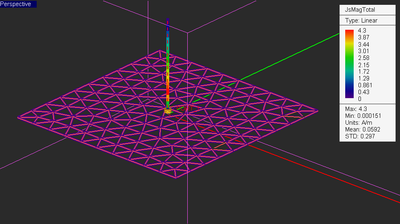
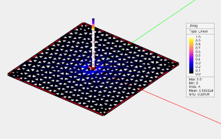
| − | At the end of a MoM3D simulation, EM.CUBE's Wire MoM engine generates a number of output data files that contain all the computed simulation data. The main output data are the current distributions and far fields. You can easily examine the 3-D color-coded intensity plots of current distributions in the Project Workspace. Current distributions are visualized on all the wires and the magnitude and phase of the electric currents are plotted for all the PEC objects. In order to view these currents, you must first define current sensors before running the Wire MoM simulation. To do this, right click on the '''Current Distributions''' item in the '''Observables''' section of the Navigation Tree and select '''Insert New Observable...'''. The Current Distribution Dialog opens up. Accept the default settings and close the dialog. A new current distribution node is added to the Navigation Tree. Unlike the [[Planar Module]], in the [[MoM3D Module]] you can define only one current distribution node in the Navigation Tree, which covers all the PEC object in the Project Workspace. After a Wire MoM simulation is completed, new plots are added under the current distribution node of the Navigation Tree. Separate plots are produced for the magnitude and phase of the linear wire currents. The magnitude maps are plotted on a normalized scale with the minimum and maximum values displayed in the legend box. The phase maps are plotted in radians between -π and π. | + | At the end of a MoM3D simulation, [[EM.Cube|EM.CUBE]]'s Wire MoM engine generates a number of output data files that contain all the computed simulation data. The main output data are the current distributions and far fields. You can easily examine the 3-D color-coded intensity plots of current distributions in the Project Workspace. Current distributions are visualized on all the wires and the magnitude and phase of the electric currents are plotted for all the PEC objects. In order to view these currents, you must first define current sensors before running the Wire MoM simulation. To do this, right click on the '''Current Distributions''' item in the '''Observables''' section of the Navigation Tree and select '''Insert New Observable...'''. The Current Distribution Dialog opens up. Accept the default settings and close the dialog. A new current distribution node is added to the Navigation Tree. Unlike the [[Planar Module]], in the [[MoM3D Module]] you can define only one current distribution node in the Navigation Tree, which covers all the PEC object in the Project Workspace. After a Wire MoM simulation is completed, new plots are added under the current distribution node of the Navigation Tree. Separate plots are produced for the magnitude and phase of the linear wire currents. The magnitude maps are plotted on a normalized scale with the minimum and maximum values displayed in the legend box. The phase maps are plotted in radians between -π and π. |
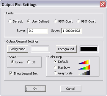
Current distribution maps are displayed with some default settings and options. You can customize the individual maps (total, magnitude, phase, etc.). To do so, open the '''Output Plot Settings Dialog''' by right clicking on the specific plot entry in the Navigation Tree and selecting '''Properties...''' or by double clicking on the surface of the plot's legend box. Two '''scale''' options are available: '''Linear''' and '''dB'''. With the '''Linear''' (default) option selected, the current value is always normalized to the maximum total current in that plane, and the normalized scale is mapped between the minimum and maximum values. If the '''dB''' option is selected, the normalized current is converted to dB scale. The plot limits (bounds) can be set individually for every current distribution plot. In the '''Limits''' section of the plot's property dialog, you see four options: '''Default''', '''User Defined''', '''95% Conf.''' and '''95% Conf.'''. Select the user defined option and enter new values for the '''Lower''' and '''Upper''' limits. The last two options are used to remove the outlier data within the 95% and 99% confidence intervals, respectively. In other words, the lower and upper limits are set to ? ± 1.96? and ? ± 2.79? , respectively, assuming a normal distribution of the data. Three color maps are offered: '''Default''', '''Rainbow''' and '''Grayscale'''. You can hide the legend box by deselecting the box labeled '''Show Legend Box'''. You can also change the foreground and background colors of the legend box. | Current distribution maps are displayed with some default settings and options. You can customize the individual maps (total, magnitude, phase, etc.). To do so, open the '''Output Plot Settings Dialog''' by right clicking on the specific plot entry in the Navigation Tree and selecting '''Properties...''' or by double clicking on the surface of the plot's legend box. Two '''scale''' options are available: '''Linear''' and '''dB'''. With the '''Linear''' (default) option selected, the current value is always normalized to the maximum total current in that plane, and the normalized scale is mapped between the minimum and maximum values. If the '''dB''' option is selected, the normalized current is converted to dB scale. The plot limits (bounds) can be set individually for every current distribution plot. In the '''Limits''' section of the plot's property dialog, you see four options: '''Default''', '''User Defined''', '''95% Conf.''' and '''95% Conf.'''. Select the user defined option and enter new values for the '''Lower''' and '''Upper''' limits. The last two options are used to remove the outlier data within the 95% and 99% confidence intervals, respectively. In other words, the lower and upper limits are set to ? ± 1.96? and ? ± 2.79? , respectively, assuming a normal distribution of the data. Three color maps are offered: '''Default''', '''Rainbow''' and '''Grayscale'''. You can hide the legend box by deselecting the box labeled '''Show Legend Box'''. You can also change the foreground and background colors of the legend box. | ||
| Line 367: | Line 367: | ||
=== Scattering Parameters and Port Characteristics === | === Scattering Parameters and Port Characteristics === | ||
| − | If the project structure is excited by gap sources, and one or more ports have been defined, the Wire MoM engine calculates the scattering (S) parameters of the selected ports, all based on the port impedances specified in the project's "Port Definition". If more than one port has been defined in the project, the scattering matrix of the multiport network is calculated. The S parameters are written into output ASCII data files. Since these data are complex, they are stored as '''.CPX''' files. Every file begins with a header starting with "#". The admittance (Y) and impedance (Z) parameters are also calculated and saved in complex data files with '''.CPX''' file extensions. The voltage standing wave ratio of the structure at the first port is also computed and saved to a real data '''.DAT''' file. | + | If the project structure is excited by gap sources, and one or more ports have been defined, the Wire MoM engine calculates the scattering (S) [[parameters]] of the selected ports, all based on the port impedances specified in the project's "Port Definition". If more than one port has been defined in the project, the scattering matrix of the multiport network is calculated. The S [[parameters]] are written into output ASCII data files. Since these data are complex, they are stored as '''.CPX''' files. Every file begins with a header starting with "#". The admittance (Y) and impedance (Z) [[parameters]] are also calculated and saved in complex data files with '''.CPX''' file extensions. The voltage standing wave ratio of the structure at the first port is also computed and saved to a real data '''.DAT''' file. |
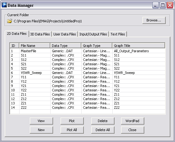
| − | You can plot the port characteristics from the Navigation Tree. Right click on the '''Port Definition''' item in the '''Observables''' section of the Navigation Tree and select one of the items: '''Plot S Parameters''', '''Plot Y Parameters''', '''Plot Z Parameters''', or '''Plot VSWR'''. In the first three cases, another sub-menu gives a list of individual port parameters. Keep in mind that in multi-port structures, each individual port parameter has its own graph. You can also see a list of all the port characteristics data files in EM.CUBE's data manager. To open data manager, click the '''Data Manager''' [[File:data_manager_icon.png]] button of the '''Compute Toolbar''' or select '''Compute [[File:larrow_tn.png]]Data Manager''' from the menu bar or right click on the '''Data Manager''' item of the Navigation Tree and select Open Data Manager... from the contextual menu or use the keyboard shortcut '''Ctrl+D'''. Select any data file by clicking and highlighting its '''ID''' in the table and then click the '''Plot''' button to plot the graph. By default, the S parameters are plotted as double magnitude-phase graphs, while the Y and Z parameters are plotted as double real-imaginary part graphs. The VSWR data are plotted on a Cartesian graph. You change the format of complex data plots. In general complex data can be plotted in three forms: | + | You can plot the port characteristics from the Navigation Tree. Right click on the '''Port Definition''' item in the '''Observables''' section of the Navigation Tree and select one of the items: '''Plot S [[Parameters]]''', '''Plot Y [[Parameters]]''', '''Plot Z [[Parameters]]''', or '''Plot VSWR'''. In the first three cases, another sub-menu gives a list of individual port [[parameters]]. Keep in mind that in multi-port structures, each individual port parameter has its own graph. You can also see a list of all the port characteristics data files in [[EM.Cube|EM.CUBE]]'s data manager. To open data manager, click the '''Data Manager''' [[File:data_manager_icon.png]] button of the '''Compute Toolbar''' or select '''Compute [[File:larrow_tn.png]]Data Manager''' from the menu bar or right click on the '''Data Manager''' item of the Navigation Tree and select Open Data Manager... from the contextual menu or use the keyboard shortcut '''Ctrl+D'''. Select any data file by clicking and highlighting its '''ID''' in the table and then click the '''Plot''' button to plot the graph. By default, the S [[parameters]] are plotted as double magnitude-phase graphs, while the Y and Z [[parameters]] are plotted as double real-imaginary part graphs. The VSWR data are plotted on a Cartesian graph. You change the format of complex data plots. In general complex data can be plotted in three forms: |
# Magnitude and Phase | # Magnitude and Phase | ||
| Line 375: | Line 375: | ||
# Smith Chart | # Smith Chart | ||
| − | In particular, it may be useful to plot the S<sub>ii</sub> parameters on a Smith chart. To change the format of a data plot, go to the row in the '''Data Manager Dialog''' that contains a specific complex data file's name and click on the fourth column under the title '''Graph Type'''. The selected table cell turns into a dropdown list that contains the above three formats. Select the desired format and click the '''Plot''' button of the data manager dialog to plot the data in the new format. | + | In particular, it may be useful to plot the S<sub>ii</sub> [[parameters]] on a Smith chart. To change the format of a data plot, go to the row in the '''Data Manager Dialog''' that contains a specific complex data file's name and click on the fourth column under the title '''Graph Type'''. The selected table cell turns into a dropdown list that contains the above three formats. Select the desired format and click the '''Plot''' button of the data manager dialog to plot the data in the new format. |
[[File:wire_pic56.png]] | [[File:wire_pic56.png]] | ||
| − | EM.CUBE's data manager showing the port characteristics data files for a two-port structure consisting of two adjacent dipoles. | + | [[EM.Cube|EM.CUBE]]'s data manager showing the port characteristics data files for a two-port structure consisting of two adjacent dipoles. |
The magnitude and phase graphs of the S<sub>11</sub> parameter. | The magnitude and phase graphs of the S<sub>11</sub> parameter. | ||
| Line 407: | Line 407: | ||
[[File:wire_pic30.png|thumb|300px|[[MoM3D Module]]'s field sensor dialog]] | [[File:wire_pic30.png|thumb|300px|[[MoM3D Module]]'s field sensor dialog]] | ||
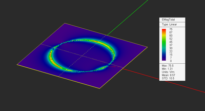
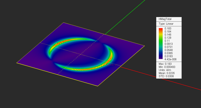
| − | EM.CUBE allows you to visualize the near fields at a specific field sensor plane. Calculation of near fields is a post-processing process and may take a considerable amount of time depending on the resolution that you specify. To define a new Field Sensor, follow these steps: | + | [[EM.Cube|EM.CUBE]] allows you to visualize the near fields at a specific field sensor plane. Calculation of near fields is a post-processing process and may take a considerable amount of time depending on the resolution that you specify. To define a new Field Sensor, follow these steps: |
* Right click on the '''Field Sensors''' item in the '''Observables''' section of the Navigation Tree and select '''Insert New Observable...''' | * Right click on the '''Field Sensors''' item in the '''Observables''' section of the Navigation Tree and select '''Insert New Observable...''' | ||
* The '''Label''' box allows you to change the sensor’s name. you can also change the color of the field sensor plane using the '''Color''' button. | * The '''Label''' box allows you to change the sensor’s name. you can also change the color of the field sensor plane using the '''Color''' button. | ||
* Set the '''Direction''' of the field sensor. This is specified by the normal vector of the sensor plane. The available options are '''X''', '''Y''' and '''Z''', with the last being the default option. | * Set the '''Direction''' of the field sensor. This is specified by the normal vector of the sensor plane. The available options are '''X''', '''Y''' and '''Z''', with the last being the default option. | ||
| − | * By default EM.CUBE creates a field sensor plane passing through the origin of coordinates (0,0,0) and coinciding with the XY plane. You can change the location of the sensor plane to any point by typing in new values for the X, Y and Z '''Center Coordinates'''. You can also changes these coordinates using the spin buttons. Keep in mind that you can move a sensor plane only along the specified direction of the sensor. Therefore, only one coordinate can effectively be changed. As you increment or decrement this coordinate, you can observe the sensor plane moving along that direction in the Project Workspace. | + | * By default [[EM.Cube|EM.CUBE]] creates a field sensor plane passing through the origin of coordinates (0,0,0) and coinciding with the XY plane. You can change the location of the sensor plane to any point by typing in new values for the X, Y and Z '''Center Coordinates'''. You can also changes these coordinates using the spin buttons. Keep in mind that you can move a sensor plane only along the specified direction of the sensor. Therefore, only one coordinate can effectively be changed. As you increment or decrement this coordinate, you can observe the sensor plane moving along that direction in the Project Workspace. |
* The initial size of the sensor plane is 100 × 100 project units. You can change the dimensions of the sensor plane to any desired size. You can also set the '''Number of Samples''' along the different directions. These determine the resolution of near field calculations. Keep in mind that large numbers of samples may result in long computation times. | * The initial size of the sensor plane is 100 × 100 project units. You can change the dimensions of the sensor plane to any desired size. You can also set the '''Number of Samples''' along the different directions. These determine the resolution of near field calculations. Keep in mind that large numbers of samples may result in long computation times. | ||
| Line 447: | Line 447: | ||
=== Modeling Antenna Arrays === | === Modeling Antenna Arrays === | ||
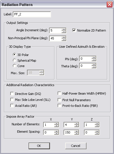
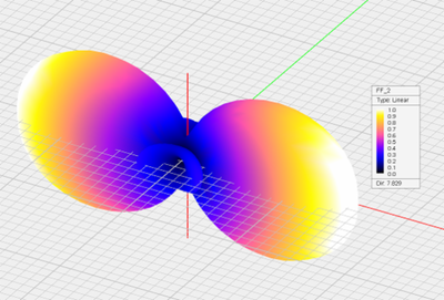
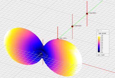
| − | In view of far field characteristics, EM.CUBE can handle antenna arrays in two different ways. The first approach is full-wave and requires building an array of radiating elements using the '''Array Tool''' and feeding individual array elements using some type of excitation. This method is very accurate and takes into account all the inter-element coupling effects. At the end of the Wire MoM simulation of the array structure, you can plot the radiation patterns and other far field characteristics of the antenna array just like any other wire-frame structure. The second approach is based on the "Array Factor" concept and ignores any inter-element coupling effects. In this approach, you can regard the structure in the project workspace as a single radiating element. A specified array factor can be calculated and multiplied by the element pattern to estimate the radiation pattern of the overall radiating array. To define an array factor, open the '''Radiation Pattern Dialog''' of the project. In the section titled '''Impose Array Factor''', you will see a default value of 1 for the '''Number of Elements''' along the three X, Y and Z directions. This implies a single radiator, which is your structure in the project workspace. There are also default zero values for the '''Element Spacing''' along the X, Y and Z directions. You should change both the number of elements and element spacing in the X, Y or Z directions to define any desired finite array lattice. For example, you can define a linear array by setting the number of elements to 1 in two directions and entering a larger value for the number of elements along the third direction. | + | In view of far field characteristics, [[EM.Cube|EM.CUBE]] can handle antenna arrays in two different ways. The first approach is full-wave and requires building an array of radiating elements using the '''Array Tool''' and feeding individual array elements using some type of excitation. This method is very accurate and takes into account all the inter-element coupling effects. At the end of the Wire MoM simulation of the array structure, you can plot the radiation patterns and other far field characteristics of the antenna array just like any other wire-frame structure. The second approach is based on the "Array Factor" concept and ignores any inter-element coupling effects. In this approach, you can regard the structure in the project workspace as a single radiating element. A specified array factor can be calculated and multiplied by the element pattern to estimate the radiation pattern of the overall radiating array. To define an array factor, open the '''Radiation Pattern Dialog''' of the project. In the section titled '''Impose Array Factor''', you will see a default value of 1 for the '''Number of Elements''' along the three X, Y and Z directions. This implies a single radiator, which is your structure in the project workspace. There are also default zero values for the '''Element Spacing''' along the X, Y and Z directions. You should change both the number of elements and element spacing in the X, Y or Z directions to define any desired finite array lattice. For example, you can define a linear array by setting the number of elements to 1 in two directions and entering a larger value for the number of elements along the third direction. |
| − | The radiation patterns of antenna arrays usually have a main beam and several side lobes. Some parameters of interest in such structures include the '''Half Power Beam Width (HPBW)''', '''Maximum Side Lobe Level (SLL)''' and '''First Null Parameters''' such as first null level and first null beam width. You can have EM.CUBE calculate all such parameters if you check the relevant boxes in the "Additional Radiation Characteristics" section of the '''Radiation Pattern Dialog'''. These quantities are saved into ASCII data files of similar names with '''.DAT''' file extensions. In particular, you can plot such data files at the end of a sweep simulation. | + | The radiation patterns of antenna arrays usually have a main beam and several side lobes. Some [[parameters]] of interest in such structures include the '''Half Power Beam Width (HPBW)''', '''Maximum Side Lobe Level (SLL)''' and '''First Null [[Parameters]]''' such as first null level and first null beam width. You can have [[EM.Cube|EM.CUBE]] calculate all such [[parameters]] if you check the relevant boxes in the "Additional Radiation Characteristics" section of the '''Radiation Pattern Dialog'''. These quantities are saved into ASCII data files of similar names with '''.DAT''' file extensions. In particular, you can plot such data files at the end of a sweep simulation. |
| − | {{Note|Defining an array factor in the radiation pattern dialog simply performs a post-processing calculation. The resulting far field obviously do not take into account any inter-element coupling effects as EM.CUBE does not construct a real physical array in the project workspace.}} | + | {{Note|Defining an array factor in the radiation pattern dialog simply performs a post-processing calculation. The resulting far field obviously do not take into account any inter-element coupling effects as [[EM.Cube|EM.CUBE]] does not construct a real physical array in the project workspace.}} |
{{Note|Using an array factor for far field calculation, you cannot assign non-uniform amplitude or phase distribution to the array elements. For this purpose, you have to define an array object.}} | {{Note|Using an array factor for far field calculation, you cannot assign non-uniform amplitude or phase distribution to the array elements. For this purpose, you have to define an array object.}} | ||
| Line 467: | Line 467: | ||
[[File:wire_pic49.png|thumb|300px|[[MoM3D Module]]'s RCS dialog]] | [[File:wire_pic49.png|thumb|300px|[[MoM3D Module]]'s RCS dialog]] | ||
| − | When the wire-frame structure is excited by a plane wave source, the calculated far field data indeed represent the scattered fields. EM.CUBE calculates the radar cross section (RCS) of a target, which is defined in the following manner: | + | When the wire-frame structure is excited by a plane wave source, the calculated far field data indeed represent the scattered fields. [[EM.Cube|EM.CUBE]] calculates the radar cross section (RCS) of a target, which is defined in the following manner: |
:<math> \sigma = 4\pi R^2 \cdot \frac{|E_{scat}|^2}{|E_{inc}|^2} </math> | :<math> \sigma = 4\pi R^2 \cdot \frac{|E_{scat}|^2}{|E_{inc}|^2} </math> | ||
<!--[[File:rcs_equation.png]]--> | <!--[[File:rcs_equation.png]]--> | ||
| − | EM.CUBE calculates three RCS quantities: the φ and θ components of the radar cross section as well as the total radar cross section: σ<sub>θ</sub>, σ<sub>φ</sub>, and σ<sub>tot</sub>. In addition, EM.CUBE [[MoM3D Module]] calculates two types of RCS for each structure: '''Bi-Static RCS''' and '''Mono-Static RCS'''. In bi-static RCS, the structure is illuminated by a plane wave at incidence angles θ<sub>0</sub> and φ<sub>0</sub> and the RCS is measured and plotted at all θ and φ angles. In mono-static RCS, the structure is illuminated by a plane wave at incidence angles θ<sub>0</sub> and φ<sub>0</sub> and the RCS is measured and plotted at the echo angles 180°-θ<sub>0</sub> and φ<sub>0</sub>.It is clear that in the case of mono-static RCS, the Wire MoM simulation engine runs an internal angular sweep, whereby the values of the plane wave incidence angles θ<sub>0</sub> and φ<sub>0</sub> are varied over the intervals [0°, 180°] and [0°, 360°], respectively, and the backscatter RCS is recorded. | + | [[EM.Cube|EM.CUBE]] calculates three RCS quantities: the φ and θ components of the radar cross section as well as the total radar cross section: σ<sub>θ</sub>, σ<sub>φ</sub>, and σ<sub>tot</sub>. In addition, [[EM.Cube|EM.CUBE]] [[MoM3D Module]] calculates two types of RCS for each structure: '''Bi-Static RCS''' and '''Mono-Static RCS'''. In bi-static RCS, the structure is illuminated by a plane wave at incidence angles θ<sub>0</sub> and φ<sub>0</sub> and the RCS is measured and plotted at all θ and φ angles. In mono-static RCS, the structure is illuminated by a plane wave at incidence angles θ<sub>0</sub> and φ<sub>0</sub> and the RCS is measured and plotted at the echo angles 180°-θ<sub>0</sub> and φ<sub>0</sub>.It is clear that in the case of mono-static RCS, the Wire MoM simulation engine runs an internal angular sweep, whereby the values of the plane wave incidence angles θ<sub>0</sub> and φ<sub>0</sub> are varied over the intervals [0°, 180°] and [0°, 360°], respectively, and the backscatter RCS is recorded. |
To calculate RCS, first you have to define an RCS observable instead of a radiation pattern. Right click on the '''Far Fields''' item in the '''Observables''' section of the Navigation Tree and select '''Insert New RCS...''' to open the Radar Cross Section Dialog. Use the '''Label''' box to change the name of the far field or change the color of the far field box using the '''Color''' button. Select the type of RCS from the two radio buttons labeled '''Bi-Static RCS''' and '''Mono-Static RCS'''. The former is the default choice. The resolution of RCS calculation is specified by '''Angle Increment''' expressed in degrees. By default, the θ and φ angles are incremented by 5 degrees. At the end of a Wire MoM simulation, besides calculating the RCS data over the entire (spherical) 3-D space, a number of 2-D RCS graphs are also generated. These are RCS cuts at certain planes, which include the three principal XY, YZ and ZX planes plus one additional constant φ-cut. This latter cut is at φ=45° by default. You can assign another phi angle in degrees in the box labeled '''Non-Principal Phi Plane'''. | To calculate RCS, first you have to define an RCS observable instead of a radiation pattern. Right click on the '''Far Fields''' item in the '''Observables''' section of the Navigation Tree and select '''Insert New RCS...''' to open the Radar Cross Section Dialog. Use the '''Label''' box to change the name of the far field or change the color of the far field box using the '''Color''' button. Select the type of RCS from the two radio buttons labeled '''Bi-Static RCS''' and '''Mono-Static RCS'''. The former is the default choice. The resolution of RCS calculation is specified by '''Angle Increment''' expressed in degrees. By default, the θ and φ angles are incremented by 5 degrees. At the end of a Wire MoM simulation, besides calculating the RCS data over the entire (spherical) 3-D space, a number of 2-D RCS graphs are also generated. These are RCS cuts at certain planes, which include the three principal XY, YZ and ZX planes plus one additional constant φ-cut. This latter cut is at φ=45° by default. You can assign another phi angle in degrees in the box labeled '''Non-Principal Phi Plane'''. | ||
| − | At the end of a Wire MoM simulation, the thee RCS plots σ<sub>θ</sub>, σ<sub>φ</sub>, and σ<sub>tot</sub>are added under the far field section of the Navigation Tree. These plots are very similar to the three 3-D radiation pattern plots. You can view them by clicking on their names in the navigation tree. The RCS values are expressed in m<sup>2</sup>. For visualization purposes, the 3-D plots are normalized to the maximum RCS value, which is also displayed in the legend box. The 2-D RCS graphs can be plotted from EM.CUBE's data manager exactly in the same way that you plot 2-D radiation pattern graphs. A total of eight 2-D RCS graphs are available: 4 polar and 4 Cartesian graphs for the XY, YZ, ZX and user defined plane cuts. At the end of a sweep simulation, EM.CUBE calculates some other quantities including the backscatter RCS (BRCS), forward-scatter RCS (FRCS) and the maximum RCS (MRCS) as functions of the sweep variable (frequency, angle, or any user defined variable). In this case, the RCS needs to be computed at a fixed pair of phi and theta angles. These angles are specified in degrees as '''User Defined Azimuth & Elevation''' in the "Output Settings" section of the '''Radar Cross Section Dialog'''. The default values of the user defined azimuth and elevation are both zero corresponding to the zenith. | + | At the end of a Wire MoM simulation, the thee RCS plots σ<sub>θ</sub>, σ<sub>φ</sub>, and σ<sub>tot</sub>are added under the far field section of the Navigation Tree. These plots are very similar to the three 3-D radiation pattern plots. You can view them by clicking on their names in the navigation tree. The RCS values are expressed in m<sup>2</sup>. For visualization purposes, the 3-D plots are normalized to the maximum RCS value, which is also displayed in the legend box. The 2-D RCS graphs can be plotted from [[EM.Cube|EM.CUBE]]'s data manager exactly in the same way that you plot 2-D radiation pattern graphs. A total of eight 2-D RCS graphs are available: 4 polar and 4 Cartesian graphs for the XY, YZ, ZX and user defined plane cuts. At the end of a sweep simulation, [[EM.Cube|EM.CUBE]] calculates some other quantities including the backscatter RCS (BRCS), forward-scatter RCS (FRCS) and the maximum RCS (MRCS) as functions of the sweep variable (frequency, angle, or any user defined variable). In this case, the RCS needs to be computed at a fixed pair of phi and theta angles. These angles are specified in degrees as '''User Defined Azimuth & Elevation''' in the "Output Settings" section of the '''Radar Cross Section Dialog'''. The default values of the user defined azimuth and elevation are both zero corresponding to the zenith. |
{{Note|Computing the 3-D mono-static RCS may take an enormous amount of computation time.}} | {{Note|Computing the 3-D mono-static RCS may take an enormous amount of computation time.}} | ||
| Line 490: | Line 490: | ||
=== Customizing 3D Plots === | === Customizing 3D Plots === | ||
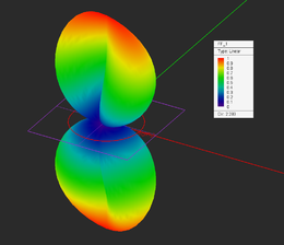
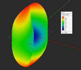
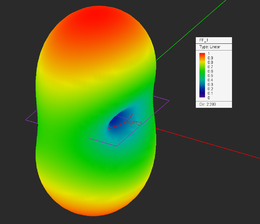
| − | Similar to the current distribution and field sensor plots, EM.CUBE's 3-D radiation pattern plots are interactive. When you move the mouse over a pattern plot, tiny dots appear on its surface. These dots correspond to the theta-phi angle pairs on the surface of the unit sphere where the far field data have been calculated. Upon mouse-over, you can highlight one of these points. A small tooltip appears on the plot that shows the normalized far field value in that direction. | + | Similar to the current distribution and field sensor plots, [[EM.Cube|EM.CUBE]]'s 3-D radiation pattern plots are interactive. When you move the mouse over a pattern plot, tiny dots appear on its surface. These dots correspond to the theta-phi angle pairs on the surface of the unit sphere where the far field data have been calculated. Upon mouse-over, you can highlight one of these points. A small tooltip appears on the plot that shows the normalized far field value in that direction. |
[[File:wire_pic41_tn.png]] | [[File:wire_pic41_tn.png]] | ||
| Line 508: | Line 508: | ||
At the end of a Wire MoM simulation, the radiation pattern data E<sub>θ</sub>, E<sub>φ</sub>, and E<sub>tot</sub> in the three principal XY, YZ and ZX planes as well as an additional user defined phi plane cut are available for plotting on 2-D graphs. There are a total of eight 2D pattern graphs in the data manager: 4 polar graphs and 4 Cartesian graphs of the same pattern data. To open data manager, click the '''Data Manager''' [[File:data_manager_icon.png]] button of the '''Compute Toolbar''' or select '''Compute [[File:larrow_tn.png]]Data Manager''' from the menu bar or right click on the '''Data Manager''' item of the Navigation Tree and select Open Data Manager... from the contextual menu or use the keyboard shortcut '''Ctrl+D'''. In the Data manager Dialog, you will see a list of all the data files available for plotting. These include the four polar pattern data files with a '''.ANG''' file extension and the four Cartesian pattern data file with a '''.DAT''' file extension. Select any data file by clicking and highlighting its '''ID''' in the table and then click the '''Plot''' button to plot the graph. | At the end of a Wire MoM simulation, the radiation pattern data E<sub>θ</sub>, E<sub>φ</sub>, and E<sub>tot</sub> in the three principal XY, YZ and ZX planes as well as an additional user defined phi plane cut are available for plotting on 2-D graphs. There are a total of eight 2D pattern graphs in the data manager: 4 polar graphs and 4 Cartesian graphs of the same pattern data. To open data manager, click the '''Data Manager''' [[File:data_manager_icon.png]] button of the '''Compute Toolbar''' or select '''Compute [[File:larrow_tn.png]]Data Manager''' from the menu bar or right click on the '''Data Manager''' item of the Navigation Tree and select Open Data Manager... from the contextual menu or use the keyboard shortcut '''Ctrl+D'''. In the Data manager Dialog, you will see a list of all the data files available for plotting. These include the four polar pattern data files with a '''.ANG''' file extension and the four Cartesian pattern data file with a '''.DAT''' file extension. Select any data file by clicking and highlighting its '''ID''' in the table and then click the '''Plot''' button to plot the graph. | ||
| − | At the end of a Wire MoM sweep simulation, other radiation characteristics are also computed as a function of the sweep variable (frequency, angle, or any other user defined variable). These include the '''Directivity (D0)''', '''Total Radiated Power (PRAD)''' and '''Directive Gain (DG)''' as a function of the theta and phi angles. Another radiation characteristic of interest especially in circularly polarized scenarios is the Axial Ratio. In EM.CUBE, the axial ratio is always defined in the LCPz or RCPz sense based on the X- and Y-components of the electric field. In order to calculate the directive gain or axial ratio, you have to check the boxes labeled '''Axial Ratio (AR)''' or '''Directive Gain (DG)''' in the "Additional Radiation Characteristics" section of the '''Radiation Pattern Dialog'''. Four 2-D Cartesian graphs of the axial ratio as functions of the theta angle a generated in the three principal XY, YZ and ZX planes as well as the additional user defined phi plane cut. At the end of a Wire MoM sweep simulation, the directive gain and axial ratio can also be plotted as functions of the sweep variable. In this case, either quantity needs to be computed at a fixed pair of phi and theta angles. These angles are specified in degrees as '''User Defined Azimuth & Elevation''' in the "Output Settings" section of the '''Radiation Pattern Dialog'''. The default values of the user defined azimuth and elevation are both zero corresponding to the zenith. | + | At the end of a Wire MoM sweep simulation, other radiation characteristics are also computed as a function of the sweep variable (frequency, angle, or any other user defined variable). These include the '''Directivity (D0)''', '''Total Radiated Power (PRAD)''' and '''Directive Gain (DG)''' as a function of the theta and phi angles. Another radiation characteristic of interest especially in circularly polarized scenarios is the Axial Ratio. In [[EM.Cube|EM.CUBE]], the axial ratio is always defined in the LCPz or RCPz sense based on the X- and Y-components of the electric field. In order to calculate the directive gain or axial ratio, you have to check the boxes labeled '''Axial Ratio (AR)''' or '''Directive Gain (DG)''' in the "Additional Radiation Characteristics" section of the '''Radiation Pattern Dialog'''. Four 2-D Cartesian graphs of the axial ratio as functions of the theta angle a generated in the three principal XY, YZ and ZX planes as well as the additional user defined phi plane cut. At the end of a Wire MoM sweep simulation, the directive gain and axial ratio can also be plotted as functions of the sweep variable. In this case, either quantity needs to be computed at a fixed pair of phi and theta angles. These angles are specified in degrees as '''User Defined Azimuth & Elevation''' in the "Output Settings" section of the '''Radiation Pattern Dialog'''. The default values of the user defined azimuth and elevation are both zero corresponding to the zenith. |
[[File:wire_pic44.png]] | [[File:wire_pic44.png]] | ||
| Line 518: | Line 518: | ||
=== 3D MoM Sweep Simulations === | === 3D MoM Sweep Simulations === | ||
| − | You can run EM.CUBE's MoM3D simulation engine in the sweep mode, whereby a parameter like frequency, plane wave angles of incidence or a user defined variable is varied over a specified range at predetermined samples. The output data are saved into data file for visualization and plotting. EM.CUBE's [[MoM3D Module]] currently offers three types of sweep: | + | You can run [[EM.Cube|EM.CUBE]]'s MoM3D simulation engine in the sweep mode, whereby a parameter like frequency, plane wave angles of incidence or a user defined variable is varied over a specified range at predetermined samples. The output data are saved into data file for visualization and plotting. [[EM.Cube|EM.CUBE]]'s [[MoM3D Module]] currently offers three types of sweep: |
# Frequency Sweep | # Frequency Sweep | ||
| Line 542: | Line 542: | ||
The [[PO Module]]'s run simulation dialog with angular sweep selected and the angle settings dialog. | The [[PO Module]]'s run simulation dialog with angular sweep selected and the angle settings dialog. | ||
| − | In a parametric sweep, one or more user defined [[variables]] are varied at the same time over their specified ranges. This creates a parametric space with the total number of samples equal to the product of the number of samples for each variable. The user defined [[variables]] are defined using EM.CUBE's '''[[Variables]] Dialog'''. For a description of EM.CUBE [[variables]], please refer to the [[CubeCAD|CUBECAD]] manual or the "Parametric Sweep" sections of the FDTD or [[Planar Module]] manuals. | + | In a parametric sweep, one or more user defined [[variables]] are varied at the same time over their specified ranges. This creates a parametric space with the total number of samples equal to the product of the number of samples for each variable. The user defined [[variables]] are defined using [[EM.Cube|EM.CUBE]]'s '''[[Variables]] Dialog'''. For a description of [[EM.Cube|EM.CUBE]] [[variables]], please refer to the [[CubeCAD|CUBECAD]] manual or the "Parametric Sweep" sections of the FDTD or [[Planar Module]] manuals. |
=== Animation of MoM3D Data === | === Animation of MoM3D Data === | ||
| − | At the end of a frequency, angular or parametric sweep simulation in EM.CUBE's [[MoM3D Module]], the output data are saved for visualization and plotting. In particular, if you have defined current distribution, field sensor or far field observables in your project, multiple 3-D plots as many as the total number of sweep samples are added to the Navigation Tree. In a single simulation run, a total of 7 current distribution plots, 14 field sensor plot and 3 radiation pattern plots or 3 RCS plots are generated under every observable node defined in the navigation tree. However, after a sweep simulation, only one plot is saved for each sweep sample. This is done to keep the resulting plots manageable. Thus, only the magnitude of the total wire currents '''|J<sub>L</sub>|''' and the total radiation pattern or total RCS are saved for each sweep sample. In the case of a field sensor observable, you have the choice to save either the total E-field magnitude plot or the total H-field magnitude plot. To change this, open the '''Field Sensor Dialog''' by right clicking on a field sensor's name in the Navigation Tree and selecting '''Properties...''' from the contextual menu. In the '''Field Display - Multiple Plots''' section of this dialog, select one of the radio sensors labeled '''E-Field''' or '''H-Field''' From this dialog, you can also choose the type of 3-D field plot for animation. The options are '''Confetti''' or '''Cone'''. | + | At the end of a frequency, angular or parametric sweep simulation in [[EM.Cube|EM.CUBE]]'s [[MoM3D Module]], the output data are saved for visualization and plotting. In particular, if you have defined current distribution, field sensor or far field observables in your project, multiple 3-D plots as many as the total number of sweep samples are added to the Navigation Tree. In a single simulation run, a total of 7 current distribution plots, 14 field sensor plot and 3 radiation pattern plots or 3 RCS plots are generated under every observable node defined in the navigation tree. However, after a sweep simulation, only one plot is saved for each sweep sample. This is done to keep the resulting plots manageable. Thus, only the magnitude of the total wire currents '''|J<sub>L</sub>|''' and the total radiation pattern or total RCS are saved for each sweep sample. In the case of a field sensor observable, you have the choice to save either the total E-field magnitude plot or the total H-field magnitude plot. To change this, open the '''Field Sensor Dialog''' by right clicking on a field sensor's name in the Navigation Tree and selecting '''Properties...''' from the contextual menu. In the '''Field Display - Multiple Plots''' section of this dialog, select one of the radio sensors labeled '''E-Field''' or '''H-Field''' From this dialog, you can also choose the type of 3-D field plot for [[animation]]. The options are '''Confetti''' or '''Cone'''. |
[[File:wire_pic60.png]] | [[File:wire_pic60.png]] | ||
| Line 552: | Line 552: | ||
Selecting control-type H-Field plot for sweep data visualization in the field sensor dialog. | Selecting control-type H-Field plot for sweep data visualization in the field sensor dialog. | ||
| − | Once the sweep simulation is finished, you can click any of the field plots and visualize it in the main window. You can also animate these field plots. Animation in EM.CUBE consists of consecutive display of the plots in the main window at a preset speed. To animate the field sensor plots, right click on the field sensor's name in the Navigation Tree and select '''Animation''' from the contextual menu. The field plots start to animate beginning with the first sample, going through all the plots one by one until the last one and repeating the loop all over again. While the animation proceeds in the main window, a dialog titled '''Animation Controls''' pops up at the lower right corner of the screen. You can drag this dialog anywhere in the project workspace from its title bar. The controls dialog shows the title of each graph as it is reviewed. You can set the speed of animation by typing in a value for '''Rate''', which is indeed the frame duration expressed in multiples of 100 milliseconds. The default frame duration is 300 msec. You can pause the animation and resume at any time. You can rewind to the first sample or skip to the last sample. You can also step through the samples one at a time using the increment (forward) or decrement (backward) buttons. To stop animation at any time, use the keyboard's '''Esc Key''' or click the '''Close (X)''' button of the animation controls dialog. | + | Once the sweep simulation is finished, you can click any of the field plots and visualize it in the main window. You can also animate these field plots. [[Animation]] in [[EM.Cube|EM.CUBE]] consists of consecutive display of the plots in the main window at a preset speed. To animate the field sensor plots, right click on the field sensor's name in the Navigation Tree and select '''[[Animation]]''' from the contextual menu. The field plots start to animate beginning with the first sample, going through all the plots one by one until the last one and repeating the loop all over again. While the [[animation]] proceeds in the main window, a dialog titled '''[[Animation]] Controls''' pops up at the lower right corner of the screen. You can drag this dialog anywhere in the project workspace from its title bar. The controls dialog shows the title of each graph as it is reviewed. You can set the speed of [[animation]] by typing in a value for '''Rate''', which is indeed the frame duration expressed in multiples of 100 milliseconds. The default frame duration is 300 msec. You can pause the [[animation]] and resume at any time. You can rewind to the first sample or skip to the last sample. You can also step through the samples one at a time using the increment (forward) or decrement (backward) buttons. To stop [[animation]] at any time, use the keyboard's '''Esc Key''' or click the '''Close (X)''' button of the [[animation]] controls dialog. |
[[File:wire_pic61_tn.png|800px]] | [[File:wire_pic61_tn.png|800px]] | ||
| − | The animation controls dialog and animation of the H-field plots of a two adjacent dipoles after a frequency sweep. | + | The [[animation]] controls dialog and [[animation]] of the H-field plots of a two adjacent dipoles after a frequency sweep. |
[[File:wire_pic62_tn.png|800px]] | [[File:wire_pic62_tn.png|800px]] | ||
| − | Animation of the wire current plots of a two adjacent dipoles after a frequency sweep. | + | [[Animation]] of the wire current plots of a two adjacent dipoles after a frequency sweep. |
Revision as of 20:14, 19 August 2014
EM.Libera is a 3D free-space structure simulator for modeling metallic structures. It features a full-wave Method of Moments (MoM) engine for analyzing wire structures or wire-frame models of metallic surfaces and solids. Many RF systems utilize wire antennas like dipoles, monopoles, loops, or arrays of wire antennas. The 3D method of moments (MoM) based on Pocklington's integral equation can accurately model such antennas and their coupling effects. Moreover, in many applications, metallic surface or solid objects can be approximately modeled as wire-frame structures. EM.Libera's Wire MoM simulator can provide an adequate numerical solution of wire-frame structures. Examples of this sort are wire antennas in the presence of large reflectors or scatterers. Wire-frame models also make a good approximation of metallic target structures for radar cross section (RCS) analysis.
EM.Libera's Wire MoM simulator is seamlessly interfaced with EM.CUBE's other simulation engines. The solution of a wire-frame structure can be imported to EM.Cube's other modules as a set of short dipole sources with proper amplitudes and phases.
Contents
A 3D Method Of Moments Primer
The Method of Moments (MoM) is a rigorous, full-wave, numerical technique for solving open boundary electromagnetic problems. Using this technique, you can analyze electromagnetic radiation, scattering and wave propagation problems with relatively short computation times and modest computing resources. The method of moments is an integral equation technique; it solves the integral form of Maxwell’s equations as opposed to their differential forms used in the finite element or finite difference time domain methods.
In a 3D MoM simulation, the currents or fields on the surface of a structure are the unknowns of the problem. The given structure is immersed in the free space. These currents or fields are discretized as a collection of elementary currents or fields with small finite spatial extents. Such elementary currents or fields are called basis functions. They obviously have a vectorial nature and must satisfy Maxwell's equations and relevant boundary conditions individually. The actual currents or fields on the surface of the given structure (the solution of the problem) are expressed as a superposition of these elementary currents or fields with initially unknown amplitudes. Through the MoM solution, you find these unknown amplitudes, from which you can then calculate the currents or fields everywhere in the structure.
EM.Cube’s MoM3D module offers two distinct 3D MoM simulation engine. The first one is a Wire MoM solver that can be used to simulate wireframe models of metallic structures. This solver is particularly useful for modeling wire-type antennas and arrays. The second engine features a powerful surface MoM solver. It can model metallic surfaces and solids as well as solid dielectric objects. The Surface MoM solver uses a surface integral equation formulation of Maxwell's equations. In the case of solid dielectric objects, equivalent electric and magnetic currents are assumed on the surface of the dielectric object to formulate the interior and exterior boundary value problems.
Free Space Green’s Function
The Green’s functions are the analytical solutions of boundary value problems when they are excited by an elementary source. This is usually an infinitesimally small vectorial point source. In order for the Green’s functions to be computationally useful, they must have analytical closed forms. This can be a mathematical expression or a more complex recursive process. It is no surprise that only very few electromagnetic boundary value problems have closed-form Green’s functions. The total electric (E) field can be expressed in terms of the electric current in the following way:
- [math] \mathbf{E = E^{inc}} + \mathbf{\iiint_V \overline{\overline{G}}_{EJ}(r|r') \cdot J(r') } d \nu' + \mathbf{\iiint_V \overline{\overline{G}}_{EM}(r|r') \cdot M(r') } d \nu' [/math]
- [math] \mathbf{H = H^{inc}} + \mathbf{\iiint_V \overline{\overline{G}}_{HJ}(r|r') \cdot J(r') } d \nu' + \mathbf{\iiint_V \overline{\overline{G}}_{HM}(r|r') \cdot M(r') } d \nu' [/math]
where is the dyadic Green’s functions for electric fields due to electric current sources and Ei is the incident or impressed electric field. The incident or impressed field provides the excitation of the structure. It may come from an incident plane wave or a gap source on a line, etc. The simplest background structure is the unbounded free space, which is represented by the following Green’s function:
- [math] \mathbf{ \overline{\overline{G}}_{EJ}(r|r') = (\overline{\overline{I}} + \nabla\nabla) } G_{\Lambda} (\mathbf{r|r'}), \quad G_{\Lambda} (\mathbf{r|r'}) = \frac{ e^{-jk_0 \mathbf{|r-r'|}} }{ 4\pi \mathbf{|r-r'|} } [/math]
where [math]\mathbf{\overline{\overline{I}}}[/math] is the unit dyad, [math]\nabla[/math] is the gradient operator, r and r' are the position vectors of the observation and source points, respectively, and k0 is the free-space propagation constant. This implies that electromagnetic waves propagate in free space in a spherical form away from the source. Note that the Green’s function has a singularity at the source, i.e. when r = r'. This singularity must be removed when solving the integral equations.
3D Integral Equations
In the more general formulation of the field integration equations, both electric and magnetic currents are included. In that case, the total electric and magnetic fields are given by the following equations:
- [math] \mathbf{E = E^{i}} + \mathbf{\iiint_V \overline{\overline{G}}_{EJ}(r|r') \cdot J(r') } + \mathbf{\iiint_V \overline{\overline{G}}_{EM}(r|r') \cdot M(r') } [/math]
- [math] \mathbf{H = H^{i}} + \mathbf{\iiint_V \overline{\overline{G}}_{HJ}(r|r') \cdot J(r') } + \mathbf{\iiint_V \overline{\overline{G}}_{HM}(r|r') \cdot M(r') } [/math]
The above coupled equations involve four types of dyadic Green's functions that represent the electric and magnetic field radiated by an electric or a magnetic current. The incident or impressed electric and magnetic fields Ei and Hi exist independently of the given structures and are related to each other depending on the type of excitation source.
Enforcing the boundary conditions on the integral definitions of the E and H fields results in a system of integral equations as follows:
- [math] \mathcal{L}_E(E) = \mathcal{L}_E \left( \mathbf{E = E^{i}} + \mathbf{\iiint_V \overline{\overline{G}}_{EJ}(r|r') \cdot J(r') } + \mathbf{\iiint_V \overline{\overline{G}}_{EM}(r|r') \cdot M(r') } \right) = 0 [/math]
- [math] \mathcal{L}_H(H) = \mathcal{L}_H \left( \mathbf{E = E^{i}} + \mathbf{\iiint_V \overline{\overline{G}}_{HJ}(r|r') \cdot J(r') } + \mathbf{\iiint_V \overline{\overline{G}}_{HM}(r|r') \cdot M(r') } \right) = 0 [/math]
where [math]\mathcal{L}_E(E)[/math] is the boundary value operator for the electric field and [math]\mathcal{L}_H(H)[/math] is the boundary value operator for the magnetic field. For example, they may require that the tangential components the E field vanish on perfect electric conductors. Or they may require that the tangential components the E and H fields be continuous across an aperture in a perfect ground plane. Given the fact that the dyadic Green’s functions and the incident or impressed fields are all known, one can solve the above system of integral equations to find the unknown currents J and M. Therefore, through these relationships you can easily cast the above integral equations in terms of unknown E and H fields.
Galerkin Testing
The integral equation derived in the previous section can be solved numerically by discretizing the computational domain using a proper meshing scheme. The original functional equation is reduced to a set of discretized linear algebraic equations over elementary cells. The unknown quantities are found by solving this system of linear equations, and many other parameters can be computed thereafter. This method of numerical solution of integral equations is known as the Method of Moments (MoM). In this method, the unknown electric current is represented by an expansion of basis functions as follows:
- [math] \mathbf{J(r)} = \sum_{n=1}^N {I_n}^{(J)} \mathbf{ {f_n}^{(J)}(r) }[/math]
where [math]\mathbf{ {f_n}^{(J)} }[/math] are the generalized vector basis functions for the expansion of electric currents, and [math]{I_n}^{(J)}[/math] are the unknown complex amplitudes of these basis functions, which have to be determined. Substituting these expansions yields the following discretized integral equation:
- [math] \mathcal{L}_E \left( \mathbf{E^i} +\iiint_V \mathbf{ \overline{\overline{G}}_{EJ}(r|r') } \cdot \sum_{n=1}^N {I_n}^{(J)} \mathbf{ {f_n}^{(J)}(r') } \, d\nu' \right) = 0 [/math]
In order to solve the above equation, the method of moments uses Galerkin's technique to turn it into a set of linear algebraic equations. This is accomplished by testing the above equations using the basis functions, leading to the following linear system:
- [math]\mathbf{[Z] \cdot [I] = [V]}[/math]
where
- [math] Z_{ij} = \iiint_{V_i} \mathbf{ {f_i}^{(J)}(r) } \, d\nu \cdot \iiint_{V_j} \mathbf{ \overline{\overline{G}}_{EJ}(r|r') \cdot {f_j}^{(J)}(r') } \, d\nu' [/math]
and
- [math] V_i = \iiint_{V_i} \mathbf{ {f_i}^{(J)}(r) \cdot E^i(r) } \, d\nu [/math]
Using a rooftop expansion of the currents on the wires, we can discretize the Pocklington integral equation. In order to convert the discretized integral equation into a system of linear system of algebraic equations, we use Galerkin’s testing process, in which the testing functions are chosen to be identical to the expansion basis functions. However, to avoid the source singularity at r=r’, the expansion functions are placed at the center of the wires, while the test functions are evaluated on the surface of the wires, assuming a finite non-zero radius for all wires. The solution vector [I] is then found as:
- [math]\mathbf{[I] = [Z]^{-1} \cdot [V] } [/math]
where [Z]-1 is the inverse of the impedance matrix and [V] is the excitation vector.
Pocklington’s Integral Equations for Wire Structures
Wire structures are made of linear PEC elements. These may consist of actual physical wires such as a dipole or loop antenna or a wireframe representation of a surface or solid object. In a wire structure, the unknown electric currents are one-dimensional. The integral equation is derived by forcing the tangential component of the electric field to vanish on the surface of the wire. This leads to the following simpler integral equation:
- [math] \mathbf{ \hat{I} \cdot E^i } - jk_0 Z_0 \int_C \left( G_A \mathbf{(r|r')} I(l') \mathbf{ \hat{l} \cdot \hat{l}' } + \frac{1}{{k_0}^2} \frac{\partial G_A}{\partial l} \frac{\partial I}{\partial l'} \right) \, dl' = 0 [/math]
where GA is the free space Green’s function, I(l) is the unknown linear current in the wire and C is the contour of the wire. and [math]\hat{l}'[/math] are the unit vectors along the wire contour. Note that GA has a singularity when r = r’, which must be either removed or avoided as will be explained later.
Discretization Of Wire Structures
The right choice of the basis functions that are used to represent the elementary currents is very important. It will determine the accuracy and computational efficiency of the resulting numerical solution. Rooftop basis functions are one of the more popular types of basis functions used in a variety of MoM formulations. The simplest rooftop function is the one-dimensional triangular functions defined as in the figure below:
This function provides a linear interpolation of the unknown currents or fields in one dimension. Note that the function vanishes at it two ends. This is a desirable feature for basis functions that represent electric currents on metallic wires as the current must vanish at the two ends of a wire. The total current on the wire can be approximated in a linear fashion by a set of one-dimensional rooftop functions as shown in the figure below:
This can be written as
- [math] I(l) = \sum_{n=1}^N a_n f_n(l) \mathbf{\hat{s}_n} [/math]
where l is the length coordinate along the wire with l=0 at its start point. [math]f_n(l)[/math] is the scaled and translated version of the linear basis function [math]f(l)[/math] shown in the previous figure. [math]\mathbf{\hat{s}_n}[/math] is the unit vector along wire.
Physical Structure & 3D Mesh Generation
Defining Groups Of PEC Objects
EM.Cube's MoM3D Module features two different simulation engines: Wire MoM and Surface MoM. Both simulation engines can handle metallic structures. The Wire MoM engine models metallic objects as wireframe structures, while the Surface MoM engine treats them as perfect electric conductor (PEC) surfaces. The PEC objects can be lines, curves, surfaces or solids. All the PEC objects are created under the PEC node in the Physical Structure section of the Navigation Tree. Objects are grouped together by their color. You can insert different PEC groups with different colors. A new PEC group can be defined by simply right clicking on the PEC item in the Navigation Tree and selecting Insert New PEC... from the contextual menu. A dialog for setting up the PEC properties opens up. From this dialog you can change the name of the group or its color. Note that PEC object do not have any material properties that can be edited.
Figure 1: MoM3D Module's Navigation Tree and its PEC dialog.
Defining Dielectric Objects

Of the two simulation engines of EM.Cube's MoM3D Module only the Surface MoM solver can handle dielectric objects as dielectric materials cannot be modeled by wireframe structures. Dielectric objects are created under the Dielectric node in the Physical Structure section of the Navigation Tree. They are grouped together by their color and material properties. You can insert different dielectric groups with different colors and different permittivity er and electric conductivity s. Note that a PEC object is the limiting cases of a lossy dielectric material when σ → ∞.
To define a new Dielectric group, follow these steps:
- Right click on the Dielectric item of the Navigation Tree and select Insert New Dielectric... from the contextual menu.
- Specify a Label, Color (and optional Texture) and the electromagnetic properties of the dielectric material to be created: Relative Permittivity (er) and Electric Conductivity (s).
- You may also choose from a list of preloaded material types. Click the button labeled Material to open EM.Cube's Materials dialog. Select the desired material from the list or type the first letter of a material to find it. For example, typing V selects Vacuum in the list. Once you close the dialog by clicking OK, the selected material properties fill the parameter fields automatically.
- Click the OK button of the dielectric material dialog to accept the changes and close it.
Figure: EM.Cube's material list.
Moving Objects Between Groups & Modules
By default, the last PEC group that was defined is active. The current active group is always listed in bold letters in the Navigation Tree. All the new objects are inserted under the current active group. A group can be activated with a right click on its entry in the Navigation Tree and then selecting the Active item of the contextual menu. You can move one or more selected objects to any desired PEC group. Right click on the highlighted selection and select Move To ![]() MoM3D
MoM3D ![]() from the contextual menu. This opens another sub-menu with a list of all the available PEC groups already defined in the PO Module. Select the desired PEC group, and all the selected objects will move to that group. The objects can be selected either in the project workspace, or their names can be selected from the Navigation Tree. In the latter case, make sure that you hold the keyboard's Shift Key or Ctrl Key down while selecting a PEC group's name from the contextual menu. In a similar way, you can move one or more objects from a Physical Optics PEC group to EM.CUBE's other modules. In this case, the sub-menus of the Move To
from the contextual menu. This opens another sub-menu with a list of all the available PEC groups already defined in the PO Module. Select the desired PEC group, and all the selected objects will move to that group. The objects can be selected either in the project workspace, or their names can be selected from the Navigation Tree. In the latter case, make sure that you hold the keyboard's Shift Key or Ctrl Key down while selecting a PEC group's name from the contextual menu. In a similar way, you can move one or more objects from a Physical Optics PEC group to EM.CUBE's other modules. In this case, the sub-menus of the Move To ![]() item of the contextual menu will indicate all the EM.CUBE modules that have valid groups for transfer of the select objects.
item of the contextual menu will indicate all the EM.CUBE modules that have valid groups for transfer of the select objects.
3D MoM Mesh Types
Coming Soon...
Creating & Viewing The Mesh
The MoM3D Module's method of moments solver assumes an infinite open boundary for your project's structure and uses the free space Green's functions for the background structure. As a result, the extents of the computational domain are infinite in all directions. The mesh generation process in EM.CUBE's MoM3D Module involves three steps:
- Setting the mesh properties.
- Generating the mesh.
- Verifying the mesh.
The commercial release of EM.CUBE's MoM3D Module provides a Wire MoM solver. In this simulation engine, all the metallic objects are discretized as a wire-frame structure. Wires, line and curves are discretized as polylines made up of small linear cells (segments).Surface and solid objects are discretized as a wire-frame mesh with triangular cells. The MoM3D mesh generator meshes the wires based on a specified mesh sampling rate expressed in cells/&lambda0. Curves are first polygonized and converted into Polyline Objects, whose edge lengths follow the specified mesh sampling rate. In the case of solid objects, only their surface and faces are discretized using a triangular wireframe mesh, which is regarded as a grid of interconnected wires. Two algorithms are offered for generation of a triangular wireframe mesh. The default algorithm is Regular Wireframe. This mesh generator creates wireframe elements that have almost equal edge lengths. The other algorithm is Structured Wireframe, which usually creates a very structured wireframe with a large number of aligned wireframe elements.
To view the MoM3D Module's wire-frame mesh, click on the ![]() button of the Compute Toolbar or select Menu
button of the Compute Toolbar or select Menu ![]() Compute
Compute ![]() Discretization
Discretization ![]() Shoe Mesh or use the keyboard shortcut Ctrl+M. When the wire-frame mesh is displayed in the Project Workspace, EM.CUBE's mesh view mode is enabled. In this mode, you can perform view operations like rotate view, pan, zoom, etc. However, you cannot select or move or edit objects. While the mesh view is enabled, the Show Mesh
Shoe Mesh or use the keyboard shortcut Ctrl+M. When the wire-frame mesh is displayed in the Project Workspace, EM.CUBE's mesh view mode is enabled. In this mode, you can perform view operations like rotate view, pan, zoom, etc. However, you cannot select or move or edit objects. While the mesh view is enabled, the Show Mesh ![]() button remains depressed. To get back to the Normal View mode, click this button one more time, or deselect Menu
button remains depressed. To get back to the Normal View mode, click this button one more time, or deselect Menu ![]() Compute
Compute ![]() Discretization
Discretization ![]() Show Mesh to remove its check mark or simply click the Esc Key of the keyboard."Show Mesh" generates a new mesh and displays it if there is none in the memory, or it simply displays an existing mesh in the memory. This is a useful feature because generating a wire-frame mesh may take a long time depending on the complexity and size of objects. If you change the structure or alter the mesh settings, a new mesh is always generated. You can ignore the mesh in the memory and force EM.CUBE to generate a mesh from the ground up by selecting Menu
Show Mesh to remove its check mark or simply click the Esc Key of the keyboard."Show Mesh" generates a new mesh and displays it if there is none in the memory, or it simply displays an existing mesh in the memory. This is a useful feature because generating a wire-frame mesh may take a long time depending on the complexity and size of objects. If you change the structure or alter the mesh settings, a new mesh is always generated. You can ignore the mesh in the memory and force EM.CUBE to generate a mesh from the ground up by selecting Menu ![]() Compute
Compute ![]() Discretization
Discretization ![]() Regenerate Mesh or by right clicking on the 3-D Mesh item of the Navigation Tree and selecting Regenerate from the contextual menu.
Regenerate Mesh or by right clicking on the 3-D Mesh item of the Navigation Tree and selecting Regenerate from the contextual menu.
The regular wireframe mesh of a PEC sphere.
Customizing the Mesh

To set the wire-frame mesh properties, click on the ![]() button of the Compute Toolbar or select Menu
button of the Compute Toolbar or select Menu ![]() Compute
Compute ![]() Discretization
Discretization ![]() Mesh Settings...or right click on the 3-D Mesh item in the Discretization section or the Navigation Tree and select Mesh Settings... from the contextual menu. The MoM3D Mesh Settings Dialog opens up. You can change the mesh generation algorithm from the drop-down list labeled Mesh Type and select one of the two options: Regular Wireframe or Structured Wireframe. You can also set the Mesh Sampling Rate, whose default value is 20 Cells/λ0.By default, surface objects or solids are wire-framed at the mesh cell size. Therefore, each wire segment of the wire-frame mesh contains one cell. Another parameter that can affect the shape of the mesh especially in the case of solid objects is the Curvature Angle Tolerance. This parameter expressed in degrees determines the apex angle of the triangular cells of the structured mesh. Lower values of the angle tolerance will results in more pointed triangular cells.
Mesh Settings...or right click on the 3-D Mesh item in the Discretization section or the Navigation Tree and select Mesh Settings... from the contextual menu. The MoM3D Mesh Settings Dialog opens up. You can change the mesh generation algorithm from the drop-down list labeled Mesh Type and select one of the two options: Regular Wireframe or Structured Wireframe. You can also set the Mesh Sampling Rate, whose default value is 20 Cells/λ0.By default, surface objects or solids are wire-framed at the mesh cell size. Therefore, each wire segment of the wire-frame mesh contains one cell. Another parameter that can affect the shape of the mesh especially in the case of solid objects is the Curvature Angle Tolerance. This parameter expressed in degrees determines the apex angle of the triangular cells of the structured mesh. Lower values of the angle tolerance will results in more pointed triangular cells.
Four-port view of the structured wireframe mesh of a PEC sphere.
Mesh of Connected Objects
All the solid objects belonging to the same PEC group are merged together using the Boolean union operation before meshing. If your structure contains attached, interconnected or overlapping solid objects, their internal common faces are removed and only the surface of the external faces is meshed. Similarly, all the surface objects belonging to the same PEC group are merged together before meshing. However, following EM.CUBE's union rules, a solid and a surface object cannot not be "unioned" together. Therefore, their meshes will not connect even if the two objects belong to the same PEC group.
You can connect a line object to a touching surface. To connect lines to surfaces and allow for current continuity, you must make sure that the box labeled Connect Lines to Touching Surfaces is checked in the Mesh Settings Dialog. If the end of a line lies on a flat surface, EM.CUBE will detect that and create the connection automatically. However, this may not always be the case if the surface is not flat and has curvature. In such cases, you have to specifically instruct EM.CUBE to enforce the connection. An example of this case is shown in the figure below.
The line object at the top of a PEC sphere and the structure's mesh without and with proximity mesh connection enforced.
Local Mesh Control
EM.CUBE applies the global mesh sampling rate to discretize all the objects in the Project Workspace. However, you can lock the mesh sampling rate of any PEC group to a desired value different than the global rate. To do so, open the property dialog of a PEC group by right clicking on its name in the Navigation Tree and select Properties... from the contextual menu. At the bottom of the dialog, check the box labeled Lock Mesh. This will enable the Sampling Rate box, where you can set a desired value. The default value is equal to the global mesh sampling rate. Keep in mind that objects that belong to different PEC groups are not merged during the mesh generation even if they overlap or are intended to be connected to one another.
Locking the mesh sampling rate of a PEC group.
Excitation Sources
Gaps Sources On Wires
A Gap is an infinitesimally narrow discontinuity that is placed on the path of the current. In EM.Cube's MoM3D Module, a gap is used to define an excitation source in the form of an ideal voltage source. Gap sources can be placed only on Line and Polyline objects. If you want to excite a curved wire antennas such as a circular loop or helix with a gap source, first you have to convert the curve object into a polyline using EM.Cube's Polygonize Tool. The gap splits the wire into two segment with a an infinitesimally small spacing between them, across which the ideal voltage source is connected. To define a new gap source, follow these steps:
- Right click on the Gap Sources item in the Sources section of the Navigation Tree and select Insert New Source... from the contextual menu. The Gap Source Dialog opens up.
- In the Source Location section of the dialog, you will find a list of all the line and polyline objects in the Project Workspace. Select the desired line or polyline object. A gap symbol is immediately placed on the selected object.
- The box labeled Direction shows the polarity of the voltage source placed on the selected object. You have the option to select either the positive or negative direction for the source. This parameter is obviously relevant only for lumped elements of active type.
- In the case of a gap on a line object, in the box labeled Offset, enter the distance of the source from the start point of the line. This value by default is initially set to the center of the line object.
- In the case of a gap on a polyline object, first choose the Side of the polyline where you want to place the source. Then, in the box labeled Offset, enter the distance of the source from the start point of that side. By default, a gap source is placed at the center of the first side of the polyline object. You can also change the offset value using the spin buttons. If you keep pushing the spin buttons, the gap source moves from one side to the next, and its side index and offset value are adjusted automatically.
- In the Source Properties section, you can specify the Source Amplitude in Volts and the Phase in Degrees.
A gap source placed on one side of a polyline representing a polygonized circular loop.
Modeling Lumped Circuits

In EM.Cube's MoM3D Module, you can define simple lumped elements in a similar manner as gap sources. In fact, a lumped element is equivalent to an infinitesimally narrow gap that is placed in the path of the current, across which Ohm's law is enforced as a boundary condition. You can define passive RLC lumped elements or active lumped elements containing a voltage gap source. The latter case can be used to excite a wire structure and model a non-ideal voltage source with an internal resistance. Unlike the FDTD Module's single-device lumped loads that connect between two adjacent nodes, the MoM3D Module's lumped circuit represent a series-parallel combination of resistor, inductor and capacitor elements. This is shown in the figure below:
To define a new lumped element, follow these steps:
- Right click on the Lumped Elements item in the Sources section of the Navigation Tree and select Insert New Source... from the contextual menu. The Lumped Element Dialog opens up.
- In the Lumped Circuit Type select one of the two options: Passive RLC or Active with Gap Source. Choosing the latter option enables the Source Properties section of the dialog.
- In the Source Location section of the dialog, you will find a list of all the line and polyline objects in the Project Workspace. Select the desired line or polyline object. A lumped element symbol is immediately placed on the selected object.
- The box labeled Direction shows the polarity of the voltage source placed on the selected object. You have the option to select either the positive or negative direction for the source.
- In the case of a gap on a line object, in the box labeled Offset, enter the distance of the source from the start point of the line. This value by default is initially set to the center of the line object.
- In the case of a gap on a polyline object, first choose the Side of the polyline where you want to place the source. Then, in the box labeled Offset, enter the distance of the source from the start point of that side. By default, a gap source is placed at the center of the first side of the polyline object. You can also change the offset value using the spin buttons. If you keep pushing the spin buttons, the gap source moves from one side to the next, and its side index and offset value are adjusted automatically.
- In the Load Properties section, the series and shunt resistance values Rs and Rp are specified in Ohms, the series and shunt inductance values Ls and Lp are specified in nH (nanohenry), and the series and shunt capacitance values Cs and Cp are specified in pF (picofarad). The impedance of the circuit is calculated at the operating frequency of the project. Only the elements that have been checked are taken into account. By default, only the series resistor has a value of 50Σ and all other circuit elements are initially grayed out.
- If the lumped element is active and contains a gap source, the Source Properties section of the dialog becomes enabled. Here you can specify the Source Amplitude in Volts (or in Amperes in the case of PMC traces) and the Phase in degrees.
- If the workspace contains an array of line or polyline objects, the array object will be listed as an eligible object for gap source placement. A lumped element will be placed on each element of the array. All the lumped elements will have identical direction, offset, resistance, inductance and capacitance values. If you define an active lumped element, you can prescribe certain amplitude and/or phase distribution to the gap sources. The available amplitude distributions include Uniform, Binomial and Chebyshev. In the last case, you need to set a value for minimum side lobe level (SLL) in dB. You can also define Phase Progression in degrees along all three principal axes.
Defining Ports
Ports are used to order and index gap sources for S parameter calculation. They are defined in the Observables section of the Navigation Tree. Right click on the Port Definition item of the Navigation Tree and select Insert New Port Definition... from the contextual menu. The Port Definition Dialog opens up, showing the total number of existing sources in the workspace. By default, as many ports as the total number of sources are created. You can define any number of ports equal to or less than the total number of sources. This includes both gap sources and active lumped elements (which contain gap sources). In the Port Association section of this dialog, you can go over each one of the sources and associate them with a desired port. Note that you can associate more than one source with same given port. In this case, you will have a coupled port. All the coupled sources are listed as associated with a single port. However, you cannot associate the same source with more than one port. Finally, you can assign Port Impedance in Ohms. By default, all port impedances are 50Σ. The table titled Port Configuration lists all the ports and their associated sources and port impedances.
| |
In EM.CUBE you cannot assign ports to an array object, even if it contains sources on its elements. To calculate the S parameters of an antenna array, you have to construct it using individual elements, not as an array object. |
The MoM3D Module's port definition dialog.
Sources & Loads On Arrays Of Wire Radiators
If the workspace contains an array of line or polyline objects, the array object will be listed as an eligible object for gap source placement. A gap source will be placed on each element of the array. All the gap sources will have identical direction and offset. However, you can prescribe certain amplitude and/or phase distributions. The available amplitude distributions include Uniform, Binomial and Chebyshev. In the last case, you need to set a value for maximum side lobe level (SLL) in dB. You can also define Phase Progression in degrees along all three principal axes.
The MoM3D Module's gap source dialog and gaps sources defined on an array of dipole wires with binomial weight distribution and 90° phase progression.
Hertzian Dipole Sources
A short dipole provides a simple way of exciting a structure in the MoM3D Module. A short dipole source acts like an infinitesimally small ideal current source. To define a short dipole source, follow these steps:
- Right click on the Short Dipoles item in the Sources section of the Navigation Tree and select Insert New Source... from the contextual menu. The Short Dipole dialog opens up.
- In the Source Location section of the dialog, you can set the coordinate of the center of the short dipole. By default, the source is placed at the origin of the world coordinate system at (0,0,0).You can type in new coordinates or use the spin buttons to move the dipole around.
- In the Source Properties section, you can specify the Amplitude in Volts, the Phase in degrees as well as the Length of the dipole in project units.
- In the Direction Unit Vector section, you can specify the orientation of the short dipole by setting values for the components uX, uY, and uZ of the dipole's unit vector. The default values correspond to a vertical (Z-directed) short dipole. The dialog normalizes the vector components upon closure even if your component values do not satisfy a unit magnitude.
When you simulate a wire structure in the MoM3D Module, you can define a Current Distribution Observable in your project. This is used not only to visualize the current distribution in the project workspace but also to save the current solution into an ASCII data file. This data file is called "MoM.IDI" by default and has a .IDI file extension. The current data are saved as line segments representing each of the wire cells together with the complex current at the center of each cell. In the MoM3D Module, you can import the current data from an existing .IDI file to serve as a set of short dipoles for excitation. To import a wire current solution, right click on Short Dipoles item in the Sources section of the Navigation Tree and select Import Dipole Source... from the contextual menu. This opens up the standard Windows Open dialog with the file type set to .IDI. Browse your folders to find the right current data file. Once you find it, select it and click the Open button of the dialog. This will create as many short dipole sources on the PO Module's Navigation Tree as the total number of mesh cells in the Wire MoM solution. From this point on, each of the imported dipoles behave like a regular short dipole source. You can open the property dialog of each individual source and modify its parameters.
Plane Wave Sources
The wire-frame structure in the MoM3D Module can be excited by an incident plane wave. In particular, a plane wave source can be used to compute the radar cross section of a metallic target. A plane wave is defined by its propagation vector indicating the direction of incidence and its polarization. EM.CUBE's MoM3D Module provides the following polarization options:
- TMz
- TEz
- Custom Linear
- LCPz
- RCPz
The direction of incidence is defined through the θ and φ angles of the unit propagation vector in the spherical coordinate system. The values of these angles are set in degrees in the boxes labeled Theta and Phi. The default values are θ = 180° and φ = 0° representing a normally incident plane wave propagating along the -Z direction with a +X-polarized E-vector. In the TMz and TEz polarization cases, the magnetic and electric fields are parallel to the XY plane, respectively. The components of the unit propagation vector and normalized E- and H-field vectors are displayed in the dialog. In the more general case of custom linear polarization, besides the incidence angles, you have to enter the components of the unit electric Field Vector. However, two requirements must be satisfied: ê . ê = 1 and ê × k = 0 . This can be enforced using the Validate button at the bottom of the dialog. If these conditions are not met, an error message is generated. The left-hand (LCP) and right-hand (RCP) circular polarization cases are restricted to normal incidences only (θ = 180°).
To define a plane wave source follow these steps:
- Right click on the Plane Waves item in the Sources section of the Navigation Tree and select Insert New Source... The Plane wave Dialog opens up.
- In the Field Definition section of the dialog, you can enter the Amplitude of the incident electric field in V/m and its Phase in degrees. The default field Amplitude is 1 V/m with a zero Phase.
- The direction of the Plane Wave is determined by the incident Theta and Phi angles in degrees. You can also set the Polarization of the plane wave and choose from the five options described earlier. When the Custom Linear option is selected, you also need to enter the X, Y, Z components of the E-Field Vector.
| |
In the spherical coordinate system, normal plane wave incidence from the top of the domain downward corresponds to θ of 180°. |
Figure: Illuminating a metallic sphere with an obliquely incident plane wave source.
Running Wire MoM Simulations
Running A Wire MoM Analysis

Once you have set up your metal structure in EM.CUBE's MoM3D Module, have defined sources and observables and have examined the quality of the structure's wire-frame mesh, you are ready to run a simulation. To open the Run Simulation Dialog, click the Run ![]() button of the Compute Toolbar or select Menu
button of the Compute Toolbar or select Menu ![]() Compute
Compute ![]() Run...or use the keyboard shortcut Ctrl+R. To start the simulation click the Run button of this dialog. Once the Wire MoM simulation starts, a new dialog called Output Window opens up that reports the various stages of Wire MoM simulation, displays the running time and shows the percentage of completion for certain tasks during the Wire MoM simulation process. A prompt announces the completion of the Wire MoM simulation. At this time, EM.CUBE generates a number of output data files that contain all the computed simulation data. These include current distributions, near field data, far field radiation pattern data as well bi-static or mono-static radar cross sections (RCS) if the structure is excited by a plane wave source.
Run...or use the keyboard shortcut Ctrl+R. To start the simulation click the Run button of this dialog. Once the Wire MoM simulation starts, a new dialog called Output Window opens up that reports the various stages of Wire MoM simulation, displays the running time and shows the percentage of completion for certain tasks during the Wire MoM simulation process. A prompt announces the completion of the Wire MoM simulation. At this time, EM.CUBE generates a number of output data files that contain all the computed simulation data. These include current distributions, near field data, far field radiation pattern data as well bi-static or mono-static radar cross sections (RCS) if the structure is excited by a plane wave source.
You have the choice to run a Fixed Frequency simulation, which is the default choice, or run a Frequency Sweep. In the former case, the simulation will be carried out at the Center Frequency of the project. This frequency can be changed from the Frequency Dialog of the project or you can click the Frequency Settings button of the Run Dialog to open up the Frequency Settings dialog. You can change the value of Center Frequency from this dialog, too.
In case you choose Frequency Sweep, the Frequency Settings dialog gives two options for Sweep Type: Adaptive or Uniform. In a uniform sweep, equally spaced samples of the frequency are used between the Start and End frequencies. These are initially set by the project Bandwidth, but you can change their values from the Frequency Settings dialog. The default Number of Samples is 10.In the case of adaptive sweep, you have to specify the Maximum Number of Iterations as well as the Error. An adaptive sweep simulation starts with a few initial frequency samples, where the Wire MoM engine is run. Then, the intermediary samples are calculated in a progressive manner. At each iteration, the frequency samples are used to calculate a rational approximation of the S parameter response over the specified frequency range. The process stops when the error criterion is met.
Figure: The output window.
Setting Wire MoM Numerical Parameters
A Wire MoM simulation involves a number of numerical parameters that normally take default values unless you change them. You can access these parameters and change their values by clicking on the Settings button next to the "Select Engine" drop-down list in the Run Dialog. This opens up the Wire MoM Engine Settings Dialog. In the Solver section of the dialog, you can choose the type of linear solver. The current options are LU and Bi-Conjugate Gradient (BiCG). The LU solver is a direct solver and is the default option of the MoM3D Module. The BiCG solver is iterative. Once selected, you have to set a Tolerance for its convergence. You can also change the maximum number of BiCG iterations by setting a new value for Max. No. of Solver Iterations / System Size. The Wire MoM simulator is based on Pocklington's integral equation method. In this method, the wires are assumed to have a very small radius. The basis functions are placed on the axis of the "wire cylinder", while the Galerkin testing is carried out on its surface to avoid the singularity of the Green's functions. In the "Source Singularity" section of the dialog, you can specify the Wire Radius . EM.CUBE's MoM3D Module assumes an identical wire radius for all wires and wireframe structures. This radius is expressed in free space wavelengths and its default value is 0.001λ0. The value of the wire radius has a direct influence on the wire's computed reactance.
The wire MoM engine settings dialog.
Visualizing Wire Current Distributions

At the end of a MoM3D simulation, EM.CUBE's Wire MoM engine generates a number of output data files that contain all the computed simulation data. The main output data are the current distributions and far fields. You can easily examine the 3-D color-coded intensity plots of current distributions in the Project Workspace. Current distributions are visualized on all the wires and the magnitude and phase of the electric currents are plotted for all the PEC objects. In order to view these currents, you must first define current sensors before running the Wire MoM simulation. To do this, right click on the Current Distributions item in the Observables section of the Navigation Tree and select Insert New Observable.... The Current Distribution Dialog opens up. Accept the default settings and close the dialog. A new current distribution node is added to the Navigation Tree. Unlike the Planar Module, in the MoM3D Module you can define only one current distribution node in the Navigation Tree, which covers all the PEC object in the Project Workspace. After a Wire MoM simulation is completed, new plots are added under the current distribution node of the Navigation Tree. Separate plots are produced for the magnitude and phase of the linear wire currents. The magnitude maps are plotted on a normalized scale with the minimum and maximum values displayed in the legend box. The phase maps are plotted in radians between -π and π.
Current distribution maps are displayed with some default settings and options. You can customize the individual maps (total, magnitude, phase, etc.). To do so, open the Output Plot Settings Dialog by right clicking on the specific plot entry in the Navigation Tree and selecting Properties... or by double clicking on the surface of the plot's legend box. Two scale options are available: Linear and dB. With the Linear (default) option selected, the current value is always normalized to the maximum total current in that plane, and the normalized scale is mapped between the minimum and maximum values. If the dB option is selected, the normalized current is converted to dB scale. The plot limits (bounds) can be set individually for every current distribution plot. In the Limits section of the plot's property dialog, you see four options: Default, User Defined, 95% Conf. and 95% Conf.. Select the user defined option and enter new values for the Lower and Upper limits. The last two options are used to remove the outlier data within the 95% and 99% confidence intervals, respectively. In other words, the lower and upper limits are set to ? ± 1.96? and ? ± 2.79? , respectively, assuming a normal distribution of the data. Three color maps are offered: Default, Rainbow and Grayscale. You can hide the legend box by deselecting the box labeled Show Legend Box. You can also change the foreground and background colors of the legend box.
Figure: A monopole antenna connected above a PEC plate and its current distribution with the default plot settings.
Figure: The output plot settings dialog, and the current distribution of the monopole-plate structure with a user defined upper limit.
Scattering Parameters and Port Characteristics
If the project structure is excited by gap sources, and one or more ports have been defined, the Wire MoM engine calculates the scattering (S) parameters of the selected ports, all based on the port impedances specified in the project's "Port Definition". If more than one port has been defined in the project, the scattering matrix of the multiport network is calculated. The S parameters are written into output ASCII data files. Since these data are complex, they are stored as .CPX files. Every file begins with a header starting with "#". The admittance (Y) and impedance (Z) parameters are also calculated and saved in complex data files with .CPX file extensions. The voltage standing wave ratio of the structure at the first port is also computed and saved to a real data .DAT file.
You can plot the port characteristics from the Navigation Tree. Right click on the Port Definition item in the Observables section of the Navigation Tree and select one of the items: Plot S Parameters, Plot Y Parameters, Plot Z Parameters, or Plot VSWR. In the first three cases, another sub-menu gives a list of individual port parameters. Keep in mind that in multi-port structures, each individual port parameter has its own graph. You can also see a list of all the port characteristics data files in EM.CUBE's data manager. To open data manager, click the Data Manager ![]() button of the Compute Toolbar or select Compute
button of the Compute Toolbar or select Compute ![]() Data Manager from the menu bar or right click on the Data Manager item of the Navigation Tree and select Open Data Manager... from the contextual menu or use the keyboard shortcut Ctrl+D. Select any data file by clicking and highlighting its ID in the table and then click the Plot button to plot the graph. By default, the S parameters are plotted as double magnitude-phase graphs, while the Y and Z parameters are plotted as double real-imaginary part graphs. The VSWR data are plotted on a Cartesian graph. You change the format of complex data plots. In general complex data can be plotted in three forms:
Data Manager from the menu bar or right click on the Data Manager item of the Navigation Tree and select Open Data Manager... from the contextual menu or use the keyboard shortcut Ctrl+D. Select any data file by clicking and highlighting its ID in the table and then click the Plot button to plot the graph. By default, the S parameters are plotted as double magnitude-phase graphs, while the Y and Z parameters are plotted as double real-imaginary part graphs. The VSWR data are plotted on a Cartesian graph. You change the format of complex data plots. In general complex data can be plotted in three forms:
- Magnitude and Phase
- Real and Imaginary Parts
- Smith Chart
In particular, it may be useful to plot the Sii parameters on a Smith chart. To change the format of a data plot, go to the row in the Data Manager Dialog that contains a specific complex data file's name and click on the fourth column under the title Graph Type. The selected table cell turns into a dropdown list that contains the above three formats. Select the desired format and click the Plot button of the data manager dialog to plot the data in the new format.
EM.CUBE's data manager showing the port characteristics data files for a two-port structure consisting of two adjacent dipoles.
The magnitude and phase graphs of the S11 parameter.
The real and imaginary part graphs of the Z21 parameter.
The Smith chart.
Running Surface MoM Simulations
Running A Surface MoM Analysis
Coming Soon...
Setting Surface MoM Numerical Parameters
Coming Soon...
Visualizing Surface Current Distributions
Coming Soon...
Visualizing Near & Far Fields In MoM3D Module
Near Field Visualization
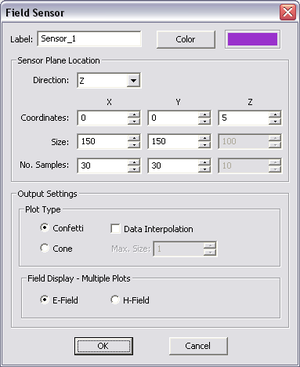
EM.CUBE allows you to visualize the near fields at a specific field sensor plane. Calculation of near fields is a post-processing process and may take a considerable amount of time depending on the resolution that you specify. To define a new Field Sensor, follow these steps:
- Right click on the Field Sensors item in the Observables section of the Navigation Tree and select Insert New Observable...
- The Label box allows you to change the sensor’s name. you can also change the color of the field sensor plane using the Color button.
- Set the Direction of the field sensor. This is specified by the normal vector of the sensor plane. The available options are X, Y and Z, with the last being the default option.
- By default EM.CUBE creates a field sensor plane passing through the origin of coordinates (0,0,0) and coinciding with the XY plane. You can change the location of the sensor plane to any point by typing in new values for the X, Y and Z Center Coordinates. You can also changes these coordinates using the spin buttons. Keep in mind that you can move a sensor plane only along the specified direction of the sensor. Therefore, only one coordinate can effectively be changed. As you increment or decrement this coordinate, you can observe the sensor plane moving along that direction in the Project Workspace.
- The initial size of the sensor plane is 100 × 100 project units. You can change the dimensions of the sensor plane to any desired size. You can also set the Number of Samples along the different directions. These determine the resolution of near field calculations. Keep in mind that large numbers of samples may result in long computation times.
After closing the Field Sensor Dialog, the a new field sensor item immediately appears under the Observables section in the Navigation Tree and can be right clicked for additional editing. Once a Wire MoM simulation is finished, a total of 14 plots are added to every field sensor node in the Navigation Tree. These include the magnitude and phase of all three components of E and H fields and the total electric and magnetic field values. Click on any of these items and a color-coded intensity plot of it will be visualized on the Project Workspace. A legend box appears in the upper right corner of the field plot, which can be dragged around using the left mouse button. The values of the magnitude plots are normalized between 0 and 1. The legend box contains the minimum field value corresponding to 0 of the color map, maximum field value corresponding to 1 of the color map, and the unit of the field quantity, which is V/m for E-field and A/m for H-field. The values of phase plots are always shown in Radians between -π and π. You can change the view of the field plot with the available view operations such as rotating, panning, zooming, etc.
Figure: A circular loop antenna fed by a gap source.
Electric and magnetic field plots of the circular loop antenna.
Visualizing 3D Radiation Patterns

Unlike the FDTD method, in the MoM3D Module you do not need a far field box to perform near-to-far-field transformations. Nonetheless, you still need to define a far field observable if you want to plot radiation patterns. A far field can be defined by right clicking on the Far Fields item in the Observables section of the Navigation Tree and selecting Insert New Radiation Pattern... from the contextual menu. The Radiation Pattern dialog opens up. You can accept most of the default settings in this dialog. The Output Settings section allows you to change the Angle Increment in the degrees, which indeed sets the resolution of far field calculations. The default value is 5 degrees. After closing the radiation pattern dialog, a far field entry immediately appears with its given name under the Far Fields item of the Navigation Tree and can be right clicked for further editing.
After a Wire MOM simulation is finished, three radiation patterns plots are added to the far field entry in the Navigation Tree. These are the far field component in Theta direction, the far field component in Phi direction and the total far field. The 3-D plots can be viewed by clicking on their name in the navigation tree. They are displayed in the Project Workspace and overlaid on the project's structure. The view of a 3-D radiation pattern plot can be changed with the available view operations such as rotate view, pan, zoom, etc. If the structure blocks the view of the pattern, you can simply hide the whole structure or parts of it. The fields are always normalized to the maximum of the total far field:
A legend box appears in the upper right corner of the 3-D radiation plot, which can be moved around by clicking and dragging with the left mouse button. The calculated Directivity of the (antenna) structure is displayed at the bottom of the legend box. It is important to note that if the wire-frame structure is excited by an incident plane wave, the radiation patterns indeed represent the far-zone scattered field data.
| |
If you do not define a far field observable in your project, no radiation patterns will be calculated at the end of a wire MoM simulation. |
| |
Every time you change the angle increment of the far field, you have to start a new simulation, even if your structure has not changed. |
3-D radiation pattern of the circular loop antenna: (Left) Theta component, (Center) Phi components, and (Right) total far field.
Modeling Antenna Arrays
In view of far field characteristics, EM.CUBE can handle antenna arrays in two different ways. The first approach is full-wave and requires building an array of radiating elements using the Array Tool and feeding individual array elements using some type of excitation. This method is very accurate and takes into account all the inter-element coupling effects. At the end of the Wire MoM simulation of the array structure, you can plot the radiation patterns and other far field characteristics of the antenna array just like any other wire-frame structure. The second approach is based on the "Array Factor" concept and ignores any inter-element coupling effects. In this approach, you can regard the structure in the project workspace as a single radiating element. A specified array factor can be calculated and multiplied by the element pattern to estimate the radiation pattern of the overall radiating array. To define an array factor, open the Radiation Pattern Dialog of the project. In the section titled Impose Array Factor, you will see a default value of 1 for the Number of Elements along the three X, Y and Z directions. This implies a single radiator, which is your structure in the project workspace. There are also default zero values for the Element Spacing along the X, Y and Z directions. You should change both the number of elements and element spacing in the X, Y or Z directions to define any desired finite array lattice. For example, you can define a linear array by setting the number of elements to 1 in two directions and entering a larger value for the number of elements along the third direction.
The radiation patterns of antenna arrays usually have a main beam and several side lobes. Some parameters of interest in such structures include the Half Power Beam Width (HPBW), Maximum Side Lobe Level (SLL) and First Null Parameters such as first null level and first null beam width. You can have EM.CUBE calculate all such parameters if you check the relevant boxes in the "Additional Radiation Characteristics" section of the Radiation Pattern Dialog. These quantities are saved into ASCII data files of similar names with .DAT file extensions. In particular, you can plot such data files at the end of a sweep simulation.
| |
Defining an array factor in the radiation pattern dialog simply performs a post-processing calculation. The resulting far field obviously do not take into account any inter-element coupling effects as EM.CUBE does not construct a real physical array in the project workspace. |
| |
Using an array factor for far field calculation, you cannot assign non-uniform amplitude or phase distribution to the array elements. For this purpose, you have to define an array object. |
Defining a finite-sized 4-element array factor in the radiation pattern dialog.
Radiation pattern of a 4-element dipole array: (Left) computed using array factor and (Right) computed by simulating an array object.
Radar Cross Section

When the wire-frame structure is excited by a plane wave source, the calculated far field data indeed represent the scattered fields. EM.CUBE calculates the radar cross section (RCS) of a target, which is defined in the following manner:
- [math] \sigma = 4\pi R^2 \cdot \frac{|E_{scat}|^2}{|E_{inc}|^2} [/math]
EM.CUBE calculates three RCS quantities: the φ and θ components of the radar cross section as well as the total radar cross section: σθ, σφ, and σtot. In addition, EM.CUBE MoM3D Module calculates two types of RCS for each structure: Bi-Static RCS and Mono-Static RCS. In bi-static RCS, the structure is illuminated by a plane wave at incidence angles θ0 and φ0 and the RCS is measured and plotted at all θ and φ angles. In mono-static RCS, the structure is illuminated by a plane wave at incidence angles θ0 and φ0 and the RCS is measured and plotted at the echo angles 180°-θ0 and φ0.It is clear that in the case of mono-static RCS, the Wire MoM simulation engine runs an internal angular sweep, whereby the values of the plane wave incidence angles θ0 and φ0 are varied over the intervals [0°, 180°] and [0°, 360°], respectively, and the backscatter RCS is recorded.
To calculate RCS, first you have to define an RCS observable instead of a radiation pattern. Right click on the Far Fields item in the Observables section of the Navigation Tree and select Insert New RCS... to open the Radar Cross Section Dialog. Use the Label box to change the name of the far field or change the color of the far field box using the Color button. Select the type of RCS from the two radio buttons labeled Bi-Static RCS and Mono-Static RCS. The former is the default choice. The resolution of RCS calculation is specified by Angle Increment expressed in degrees. By default, the θ and φ angles are incremented by 5 degrees. At the end of a Wire MoM simulation, besides calculating the RCS data over the entire (spherical) 3-D space, a number of 2-D RCS graphs are also generated. These are RCS cuts at certain planes, which include the three principal XY, YZ and ZX planes plus one additional constant φ-cut. This latter cut is at φ=45° by default. You can assign another phi angle in degrees in the box labeled Non-Principal Phi Plane.
At the end of a Wire MoM simulation, the thee RCS plots σθ, σφ, and σtotare added under the far field section of the Navigation Tree. These plots are very similar to the three 3-D radiation pattern plots. You can view them by clicking on their names in the navigation tree. The RCS values are expressed in m2. For visualization purposes, the 3-D plots are normalized to the maximum RCS value, which is also displayed in the legend box. The 2-D RCS graphs can be plotted from EM.CUBE's data manager exactly in the same way that you plot 2-D radiation pattern graphs. A total of eight 2-D RCS graphs are available: 4 polar and 4 Cartesian graphs for the XY, YZ, ZX and user defined plane cuts. At the end of a sweep simulation, EM.CUBE calculates some other quantities including the backscatter RCS (BRCS), forward-scatter RCS (FRCS) and the maximum RCS (MRCS) as functions of the sweep variable (frequency, angle, or any user defined variable). In this case, the RCS needs to be computed at a fixed pair of phi and theta angles. These angles are specified in degrees as User Defined Azimuth & Elevation in the "Output Settings" section of the Radar Cross Section Dialog. The default values of the user defined azimuth and elevation are both zero corresponding to the zenith.
| |
Computing the 3-D mono-static RCS may take an enormous amount of computation time. |
Figure: A half-wave wire connected to a metal plate illuminated by an obliquely incident plane wave.
The RCS of the wire-plate structure: (Left) σθ, (Center) σφ and (Right) total RCS..
Customizing 3D Plots
Similar to the current distribution and field sensor plots, EM.CUBE's 3-D radiation pattern plots are interactive. When you move the mouse over a pattern plot, tiny dots appear on its surface. These dots correspond to the theta-phi angle pairs on the surface of the unit sphere where the far field data have been calculated. Upon mouse-over, you can highlight one of these points. A small tooltip appears on the plot that shows the normalized far field value in that direction.
Reading far field values from a 3-D radiation pattern plot by mouse-over.
You can change the type of the 3-D radiation pattern plot through the Radiation Pattern Dialog. The plot type change applies to all the three nodes: theta component, phi component and total field patterns. In the 3D Display Type section of this dialog you can choose from three options: 3D Polar, which is the default choice, Spherical Map and Cone. In the last two cases, the far field values are plotted on the surface of the unit sphere, where each point correspond to a (θ, φ) pair. In the spherical map, the curved cells of the unit sphere are colored based on their field value. In the cone-type plot, a vectorial visualization of the far fields is generated. In the last case, you can also set the size of the cones that represent the far field vectors.
The spherical map and cone (vectorial) versions of the radiation pattern show in the previous figure.
Just like current distribution and field sensor plots, each individual 3-D radiation pattern plots has an Output Settings Dialog, from which you can further customize the plot's scale (linear vs. dB), lower and upper limits and color map type.
2D Radiation Graphs
At the end of a Wire MoM simulation, the radiation pattern data Eθ, Eφ, and Etot in the three principal XY, YZ and ZX planes as well as an additional user defined phi plane cut are available for plotting on 2-D graphs. There are a total of eight 2D pattern graphs in the data manager: 4 polar graphs and 4 Cartesian graphs of the same pattern data. To open data manager, click the Data Manager ![]() button of the Compute Toolbar or select Compute
button of the Compute Toolbar or select Compute ![]() Data Manager from the menu bar or right click on the Data Manager item of the Navigation Tree and select Open Data Manager... from the contextual menu or use the keyboard shortcut Ctrl+D. In the Data manager Dialog, you will see a list of all the data files available for plotting. These include the four polar pattern data files with a .ANG file extension and the four Cartesian pattern data file with a .DAT file extension. Select any data file by clicking and highlighting its ID in the table and then click the Plot button to plot the graph.
Data Manager from the menu bar or right click on the Data Manager item of the Navigation Tree and select Open Data Manager... from the contextual menu or use the keyboard shortcut Ctrl+D. In the Data manager Dialog, you will see a list of all the data files available for plotting. These include the four polar pattern data files with a .ANG file extension and the four Cartesian pattern data file with a .DAT file extension. Select any data file by clicking and highlighting its ID in the table and then click the Plot button to plot the graph.
At the end of a Wire MoM sweep simulation, other radiation characteristics are also computed as a function of the sweep variable (frequency, angle, or any other user defined variable). These include the Directivity (D0), Total Radiated Power (PRAD) and Directive Gain (DG) as a function of the theta and phi angles. Another radiation characteristic of interest especially in circularly polarized scenarios is the Axial Ratio. In EM.CUBE, the axial ratio is always defined in the LCPz or RCPz sense based on the X- and Y-components of the electric field. In order to calculate the directive gain or axial ratio, you have to check the boxes labeled Axial Ratio (AR) or Directive Gain (DG) in the "Additional Radiation Characteristics" section of the Radiation Pattern Dialog. Four 2-D Cartesian graphs of the axial ratio as functions of the theta angle a generated in the three principal XY, YZ and ZX planes as well as the additional user defined phi plane cut. At the end of a Wire MoM sweep simulation, the directive gain and axial ratio can also be plotted as functions of the sweep variable. In this case, either quantity needs to be computed at a fixed pair of phi and theta angles. These angles are specified in degrees as User Defined Azimuth & Elevation in the "Output Settings" section of the Radiation Pattern Dialog. The default values of the user defined azimuth and elevation are both zero corresponding to the zenith.
The data manager dialog showing a list of 2-D polar and Cartesian radiation pattern graphs.
More 3D MoM Simulation Types
3D MoM Sweep Simulations
You can run EM.CUBE's MoM3D simulation engine in the sweep mode, whereby a parameter like frequency, plane wave angles of incidence or a user defined variable is varied over a specified range at predetermined samples. The output data are saved into data file for visualization and plotting. EM.CUBE's MoM3D Module currently offers three types of sweep:
- Frequency Sweep
- Angular Sweep
- Parametric Sweep
To run a MoM3D sweep, open the Run Simulation Dialog and select one of the above sweep types from the Simulation Mode drop-down list in this dialog. If you select either frequency or angular sweep, the Settings button located next to the simulation mode drop-down list becomes enabled. If you click this button, the Frequency Settings Dialog or Angle Settings Dialog opens up, respectively. In the frequency settings dialog, you can set the start and end frequencies as well as the number of frequency samples. The start and end frequency values are initially set based on the project's center frequency and bandwidth. During a frequency sweep, as the project's frequency changes, so does the wavelength. As a result, the mesh of the structure also changes at each frequency sample. The frequency settings dialog gives you three choices regarding the mesh of the project structure during a frequency sweep:
- Fix mesh at the highest frequency.
- Fix mesh at the center frequency.
- Re-mesh at each frequency.
The MoM3D Module offers two types of frequency sweep: adaptive or uniform. In a uniform sweep, equally spaced frequency samples are generated between the start and end frequencies. In the case of an adaptive sweep, you must specify the Maximum Number of Iterations as well as the Error. An adaptive sweep simulation starts with a few initial frequency samples, where the Wire MoM engine is initially run. Then, the intermediary frequency samples are calculated and inserted in a progressive manner. At each iteration, the frequency samples are used to calculate a rational approximation of the scattering parameter response over the specified frequency range. The process stops when the specified error criterion is met in a mean-square sense. The adaptive sweep simulation results are always continuous and smooth. This is due to the fact that a rational function curve is fitted through the discrete frequency data points. This usually captures frequency response characteristics such as resonances with much fewer calculated data points. However, you have to make sure that the process converges. Otherwise, you might get an entirely wrong, but still perfectly smooth, curve at the end of the simulation.
The MoM3D Module's run simulation dialog with frequency sweep selected and the frequency settings dialog.
You can run an angular sweep only if your project has a plane wave excitation. In this case, you have to define a plane wave source with the default settings. During an angular sweep, either the incident theta angle or incident phi angle is varied within the specified range. The other angle remains fixed at the value that is specified in the Plane Wave Dialog. You have to select either Theta or Phi as the Sweep Angle in the Angle Settings Dialog. Then you can set the start and end angles as well as the number of angle samples.
The PO Module's run simulation dialog with angular sweep selected and the angle settings dialog.
In a parametric sweep, one or more user defined variables are varied at the same time over their specified ranges. This creates a parametric space with the total number of samples equal to the product of the number of samples for each variable. The user defined variables are defined using EM.CUBE's Variables Dialog. For a description of EM.CUBE variables, please refer to the CUBECAD manual or the "Parametric Sweep" sections of the FDTD or Planar Module manuals.
Animation of MoM3D Data
At the end of a frequency, angular or parametric sweep simulation in EM.CUBE's MoM3D Module, the output data are saved for visualization and plotting. In particular, if you have defined current distribution, field sensor or far field observables in your project, multiple 3-D plots as many as the total number of sweep samples are added to the Navigation Tree. In a single simulation run, a total of 7 current distribution plots, 14 field sensor plot and 3 radiation pattern plots or 3 RCS plots are generated under every observable node defined in the navigation tree. However, after a sweep simulation, only one plot is saved for each sweep sample. This is done to keep the resulting plots manageable. Thus, only the magnitude of the total wire currents |JL| and the total radiation pattern or total RCS are saved for each sweep sample. In the case of a field sensor observable, you have the choice to save either the total E-field magnitude plot or the total H-field magnitude plot. To change this, open the Field Sensor Dialog by right clicking on a field sensor's name in the Navigation Tree and selecting Properties... from the contextual menu. In the Field Display - Multiple Plots section of this dialog, select one of the radio sensors labeled E-Field or H-Field From this dialog, you can also choose the type of 3-D field plot for animation. The options are Confetti or Cone.
Selecting control-type H-Field plot for sweep data visualization in the field sensor dialog.
Once the sweep simulation is finished, you can click any of the field plots and visualize it in the main window. You can also animate these field plots. Animation in EM.CUBE consists of consecutive display of the plots in the main window at a preset speed. To animate the field sensor plots, right click on the field sensor's name in the Navigation Tree and select Animation from the contextual menu. The field plots start to animate beginning with the first sample, going through all the plots one by one until the last one and repeating the loop all over again. While the animation proceeds in the main window, a dialog titled Animation Controls pops up at the lower right corner of the screen. You can drag this dialog anywhere in the project workspace from its title bar. The controls dialog shows the title of each graph as it is reviewed. You can set the speed of animation by typing in a value for Rate, which is indeed the frame duration expressed in multiples of 100 milliseconds. The default frame duration is 300 msec. You can pause the animation and resume at any time. You can rewind to the first sample or skip to the last sample. You can also step through the samples one at a time using the increment (forward) or decrement (backward) buttons. To stop animation at any time, use the keyboard's Esc Key or click the Close (X) button of the animation controls dialog.
The animation controls dialog and animation of the H-field plots of a two adjacent dipoles after a frequency sweep.
Animation of the wire current plots of a two adjacent dipoles after a frequency sweep.
