Difference between revisions of "EM.Picasso Lesson 5: Modeling Periodic Frequency Selective Surfaces"

From Emagtech Wiki
Jump to: navigation, search
(Running a Planar MoM Analysis)
Line 161: Line 161:
  
  
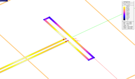
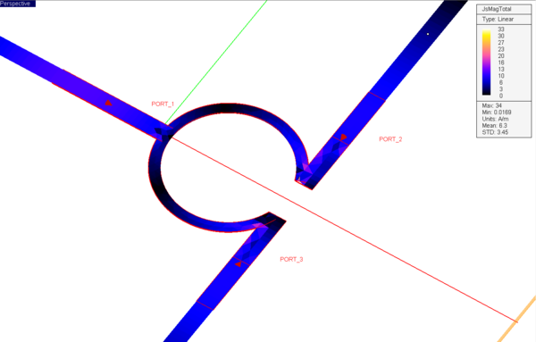
Also, visualize the current distribution on the divider circuit. Note that the maximum current on Port 1 line is about 40A/m, while the maximum current values on the Port 2 and Port 3 lines are about 28V/m (40/√2 ≅ 28).
+
Also, visualize the current distribution on the divider circuit. Note that the maximum current on Port 1 line is about 40A/m, while the maximum current values on the Port 2 and Port 3 lines are about 28V/m as expected (40 / √2 ≅ 28).
 
+
  
 
==Adding a Lumped Resistor==
 
==Adding a Lumped Resistor==

Revision as of 22:33, 27 October 2014

Tutorial Project: Designing a Microstrip Wilkinson Power Divider
Pmom lec4 9 jtot.png

Objective: In this project, you will build a slot-based planar structure using PMC traces and excite it using a pair of coupled de-embedded sources.

Concepts/Features:

  • CubeCAD
  • PMC Traces
  • De-embedded Source
  • Coupled Ports
  • Radiation Pattern
  • Adaptive Sweep

Minimum Version Required: All versions

'Download2x.png Download Link: [1]

Objective:

To construct a CPW-fed folded slot antenna in EM.Cube’s Planar Module, analyze it and visualize its near and far field characteristics and parameterize the design and explore its variations.

What You Will Learn:

In this tutorial lesson you will introduce slot (PMC) traces to your physical struture. You will also define coupled ports to model coplanar waveguide (CPW) structures.

Getting Started

Open the EM.Cube application and switch to Planar Module. Start a new project with the following attributes:

  1. Name: PMOMLesson5
  2. Length Units: mm
  3. Frequency Units: GHz
  4. Center Frequency: 2.4GHz
  5. Bandwidth: 1GHz
  6. Number of Finite Substrate Layers: 1
  7. Layer Stack-up:
  8. Top Half-Space: Vacuum
  9. Middle Layer: ROGER RT/Duroid 5880, εr = 2.2, μr = 1, σ = σm = 0, thickness = 0.787mm
  10. Bottom Half-Space: Vacuum

Drawing the Divider Structure

Create a PEC group on the Navigation Tree and call it PEC_1. Draw six rectangle strip objects with dimensions and locations given in the table below:

Label Object Type Function LCS Origin Length Width
Rect_Strip_1 Rectangle Strip 50Ω Input Line (-1.5mm, 0, 0.787mm) 5mm 2.4mm
Rect_Strip_2 Rectangle Strip 50Ω Input Line (19mm, 5mm, 0.787mm) 2.4mm 5mm
Rect_Strip_3 Rectangle Strip 50Ω Input Line (19mm, -5mm, 0.787mm) 2.4mm 5mm
Rect_Strip_4 Rectangle Strip 50Ω Port Line (-8mm, 0, 0.787mm) 8mm 2.4mm
Rect_Strip_5 Rectangle Strip 50Ω Port Line 19mm, 11.5mm, 0.787mm) 2.4mm 8mm
Rect_Strip_6 Rectangle Strip 50Ω Port Line 19mm, -11.5mm, 0.787mm) 2.4mm 8mm


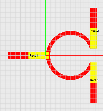
EM.Cube's "Circle Strip Tool" is very versatile, and besides circles, you can use it to draw rings and arcs. Draw a circle strip object with an "Outer Radius" of 9.65mm and an "Inner Radius" of 8.25mm. Place the local coordinate system (LCS) of the object at (10mm, 0, 0.787mm). This ring strip will serve as the two 70.7Ω quarter-wave arms of the Wilkinson power divider. Also, set the "Start Angle" and "End Angle" of the arc to 20° and 340°, respectively.


The geometry of the Wilkinson power divider without the lumped resistor.
The property dialog of the Circle Strip object.
The 50Ω input line segments of the divider structure.
The 70.7Ω arms of the divider.
The 50Ω port lines.


Defining Sources, Assigning Ports & Examining the Planar Mesh

Define three de-embedded source DS_1 (+X-directed), DS_2 (-Y-directed) and DS_3 (+Y-directed) for the three port lines Rect4, Rect5 and Rect6, respectively. Also, define a default "Port Definition" observable that assigns Ports 1, 2 and 3 to the three de-embedded source, respectively.

Open the Planar Mesh Settings dialog and change the mesh density to 30 cells per effective wavelength. Generate and view the mesh of your planar structure. Note how the three line segments Rect1, Rect2 and Rect3 have merged with the circular arc-ring, and a consistent mesh has been generated.

Attention icon.png Before generating a Planar MoM mesh, EM.Cube performs a Boolean union operation on all the objects belonging to the same trace group. All the geometrical overlaps between adjacent objects are resolved as part of meshing.


The geometry of the Wilkinson power divider with de-embedded sources and port assignments.
The planar mesh of the Wilkinson power divider without the lumped resistor .

Running a Planar MoM Analysis

The geometry of the Wilkinson power divider without the lumped resistor.

Run a quick planar MoM analysis of your three-port power divider structure. At the end of the simulation, the following S-parameter values are reported in the Output Message Window:


S11(dB): -14.158286

S21(dB): -3.119946

S31(dB): -3.194342

S22(dB): -6.227977

S33(dB): -6.094034

S32(dB): -7.046050


Also, visualize the current distribution on the divider circuit. Note that the maximum current on Port 1 line is about 40A/m, while the maximum current values on the Port 2 and Port 3 lines are about 28V/m as expected (40 / √2 ≅ 28).

Adding a Lumped Resistor

Next, you will run add a lumped resistor between the two output ports of your power divider to complete the Wilkinson design. But first you need to draw a line segment between the two objects Rect2 and Rect3. Draw a new rectangle strip object


Attention icon.png Just like gap sources, lumped elements require a host line object, and can only be defined in association with an existing rectangle strip object.


frequency sweep of your folded slot antenna to examine its frequency response and resonance behavior. Keep in mind that an adaptive frequency sweep does not generate current distribution plots or 3D radiation patterns at each frequency sample, but a uniform frequency sweep does. Therefore, first run a uniform frequency sweep with the following parameters:

Start Frequency: 1.4GHz

End Frequency: 2.0GHz

Number of Frequency Samples: 13


You will see that around 1.65GHz, the imaginary part of Z11 (i.e. input reactance) vanishes. Additionally, around the same frequency, the magnitude of S11 (return loss) dips into a deep minimum. This a good sign that your antenna both is both resonant and impedance-matched at that frequency.


The graphs of S11 as a function of frequency
The graphs of Z11 as a function of frequency


The figures below show the magnetic current distributions on the slot antenna and its CPW feed line at three different frequencies: 1.4GHz (left), 1.65GHz (middle) and 1.85GHz (right).


The magnetic current distributions on the slot antenna and its CPW feed line at 1.4GHz (left), 1.65GHz (middle) and 1.85GHz


Next, run an adaptive frequency sweep with the following parameters:

Start Frequency: 1.4GHz

End Frequency: 2.0GHz

Min No. of Frequency Samples: 5

Max No. of Frequency Samples: 15

Convergence Criterion: 0.02


At the end of the adaptive sweep, graph the data files “S11_RationalFit.CPX” and “Z11_RationalFit.CPX” in EM.Grid. From the S11 and Z11 graphs you can see that the actual resonant frequency is about 1.665GHz. You can also check the voltage standing wave ration of your antenna structure by graphing the file “VSWR_RationalFit.DAT”. In this graph, you can see the minimum VSWR value of 1.06. The two red horizontal lines mark VSWR = 1.0 and VSWR = 1.5.


The graph of S11 as a function of frequency (adaptive)
The graph of Z11 as a function of frequency (adaptive)
The plot of voltage standing wave ratio

Back to EM.Cube Wiki Main Page