Difference between revisions of "EM.Picasso Lesson 5: Modeling Periodic Frequency Selective Surfaces"
Kazem Sabet (Talk | contribs) (→Running a Planar MoM Analysis) |
Kazem Sabet (Talk | contribs) (→Running a Planar MoM Analysis) |
||
| Line 149: | Line 149: | ||
| − | |||
S11(dB): -14.158286 | S11(dB): -14.158286 | ||
| − | |||
S21(dB): -3.119946 | S21(dB): -3.119946 | ||
| − | |||
S31(dB): -3.194342 | S31(dB): -3.194342 | ||
| − | |||
S22(dB): -6.227977 | S22(dB): -6.227977 | ||
| − | |||
S33(dB): -6.094034 | S33(dB): -6.094034 | ||
| − | |||
S32(dB): -7.046050 | S32(dB): -7.046050 | ||
Revision as of 20:58, 27 October 2014
Contents
Objective:
To construct a CPW-fed folded slot antenna in EM.Cube’s Planar Module, analyze it and visualize its near and far field characteristics and parameterize the design and explore its variations.
What You Will Learn:
In this tutorial lesson you will introduce slot (PMC) traces to your physical struture. You will also define coupled ports to model coplanar waveguide (CPW) structures.
Getting Started
Open the EM.Cube application and switch to Planar Module. Start a new project with the following attributes:
- Name: PMOMLesson5
- Length Units: mm
- Frequency Units: GHz
- Center Frequency: 2.4GHz
- Bandwidth: 1GHz
- Number of Finite Substrate Layers: 1
- Layer Stack-up:
- Top Half-Space: Vacuum
- Middle Layer: ROGER RT/Duroid 5880, εr = 2.2, μr = 1, σ = σm = 0, thickness = 0.787mm
- Bottom Half-Space: Vacuum
Drawing the Divider Structure
Create a PEC group on the Navigation Tree and call it PEC_1. Draw six rectangle strip objects with dimensions and locations given in the table below:
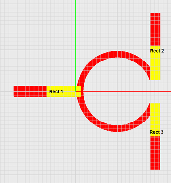
Defining Sources, Assigning Ports & Examining the Planar MeshDefine three de-embedded source DS_1 (+X-directed), DS_2 (-Y-directed) and DS_3 (+Y-directed) for the three port lines Rect4, Rect5 and Rect6, respectively. Also, define a default "Port Definition" observable that assigns Ports 1, 2 and 3 to the three de-embedded source, respectively. Open the Planar Mesh Settings dialog and change the mesh density to 30 cells per effective wavelength. Generate and view the mesh of your planar structure. Note how the three line segments Rect1, Rect2 and Rect3 have merged with the circular arc-ring, and a consistent mesh has been generated.
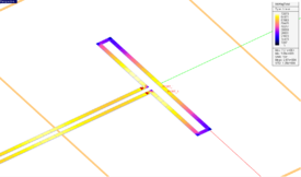
Running a Planar MoM AnalysisBefore running a simulation, let’s take a look at the planar mesh of your slot antenna. The specified mesh density for this project is 30 cells/λeff. As you would expect, both feed lines with de-embedded ports on them are extended to 2λg. For slot lines,λeff = λ0/√εeff, where εeff ≈ (εr + 1)/2, if the medium above the slot is vacuum and the one beneath it is a dielectric of permittivity εr. Here you can see a planar mesh consisting solely of rectangular cells. EM.Cube’s “Hybrid Planar Mesher” identifies the junctions and joints among rectangular objects of the same width and generates a smooth rectangular transition mesh in those areas. This happens if you create all those joints objects (L2, L3, L6, L7, L10, L11). Otherwise, if you simply connect rectangular objects from their elongated sides without paying particular attention to microstrip discontinuities like bends and tee or cross junctions, a triangular mesh will be generated at these connection areas. Results like port or radiation characteristics are usually good and comparable in both cases. However, if you are interested in detailed current distribution plots, then you need to increase the mesh density adequately in the latter case.Run a quick planar MoM analysis of your folded slot antenna and visualize its current distribution and 3D radiation pattern. Keep in mind that since your slot trace is purely PMC, the electric surface current density is zero everywhere, and you should look at the magnetic current density plots instead. Note that magnetic current density has units of V/m, which is the same as that of electric field. The radiation pattern is typical of a dipole antenna as you would expect. The port characteristics are reported as:
S21(dB): -3.119946 S31(dB): -3.194342 S22(dB): -6.227977 S33(dB): -6.094034 S32(dB): -7.046050
Running a Frequency SweepNext, you will run a frequency sweep of your folded slot antenna to examine its frequency response and resonance behavior. Keep in mind that an adaptive frequency sweep does not generate current distribution plots or 3D radiation patterns at each frequency sample, but a uniform frequency sweep does. Therefore, first run a uniform frequency sweep with the following parameters: Start Frequency: 1.4GHz End Frequency: 2.0GHz Number of Frequency Samples: 13
Start Frequency: 1.4GHz End Frequency: 2.0GHz Min No. of Frequency Samples: 5 Max No. of Frequency Samples: 15 Convergence Criterion: 0.02
|


