Objective:
To construct a probe-fed rectangular microstrip patch antenna on a conductor-backed dielectric substrate, define a proper source to model the feeding probe, and investigate different types of computational domain truncation and boundary conditions.
What You Will Learn:
In this tutorial you will use a lumped source to excite a more, namely, a plane wave. You will also introduce different materials and try out more complex geometries to build your physical structure. You learn how to plot different types of data files and perform mathematical operations on your data sets.
Getting Started
Open the EM.Cube application and switch to FDTD Module. Start a new project with the following attributes:
- Name: FDTDLesson3
- Length Units: mm
- Frequency Units: GHz
- Center Frequency: 1.575GHz
- Bandwidth: 2GHz
Creating Material Groups & Drawing Objects
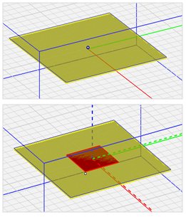
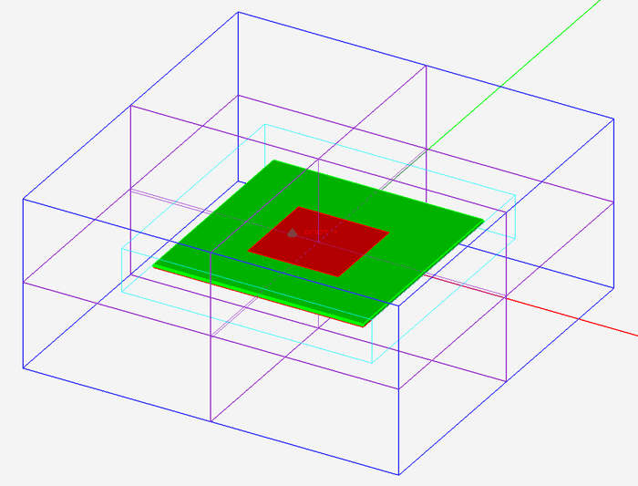
You can draw the rectangle strip first in a blank area of the project workspace and then adjust its coordinates to move it to the right location. In this case, set the coordinates of the LCS origin of the rectangle object at (0, 0, 1.524mm), i.e., at the center of the top face of the dielectric box. Or you can draw the patch right on location. Hover the mouse over the top face of the dielectric box. The mouse cursor snaps to a small highlighted “ball” at the center of box’s top face. Start drawing the rectangle right from this point.
| |
Under EM.Cube’s default Snap-To-Object mode, if you hover the mouse over an object, its color becomes translucent. In this mouse-over state, the mouse cursor snaps to one of the characteristic points of the highlighted objectobject is highlighted. You can always activate EM.Cube’s useful Snap-To-Object mode using the keyboard shortcut “O”. |
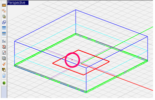
Finally, while the PEC_1 group is still active, draw a vertical line of length 1.524mm to represent the probe feed on the patch antenna. Remember to hold down the keyboard’s Shift Key when drawing the line object to make it perpendicular to the current XY work plane. Set the coordinates of the LCS origin of the line object at (-15mm, 0, 0). The line object will move underneath the metallic patch object.
Domain Settings & Boundary Conditions
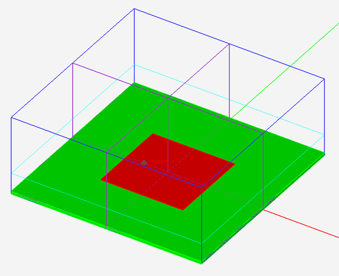
In this tutorial lesson you will simulate two different versions of your microstrip patch antenna: one with an infinite substrate and one with a finite substrate. You will see the effect of a finite substrate on the radiation characteristics of the patch antenna. EM.Cube provides CMPL boundary conditions that absorb impinging waves and thus emulate an open-boundary free space. One of the important properties of CPML boundary conditions is that they can be placed around a dielectric medium, and they equally absorb waves impinging from inside the dielectric material. This means that to the impinging wave, the CPML indeed emulated a dielectric medium of infinite extents.
| |
If a CMPL wall touches the boundary of a dielectric medium, its makes the dielectric medium look like having an infinite extent in that direction. |
Source Definition
Define a new lumped source in the “Lumped Sources” section of the Navigation Tree. This will be placed on Line_1 as it is the only eligible line object in your project. Keep the default offset, unit amplitude, zero phase and 50Ω resistance.
Defining Project Observables
For this project, you will define three observables:
1. A field sensor located at (0, 0, 1.524) coinciding with the patch plane.
2. A far field box with a “Radiation Pattern” observable.
3. A default port definition for lumped source LS_1 with a 50Ω port impedance.
By default, EM.Cube’s FDTD Module assumes a free space background medium for radiation pattern calculation. In other words, it assumes that your physical structure is immersed in the free space, and it uses the free-space Green’s functions for the near-to-far-field transformation. However, in this project, your real background structure is an infinite dielectric substrate with an infinite PEC ground plane at its bottom. FDTD Module’s Radiation Pattern Dialog currently gives four options for a ar field background medium:
1. Free Space (default)
2. PEC Ground Plane
3. PMC Ground Plane
4. Dielectric Half-Space with specified εr and
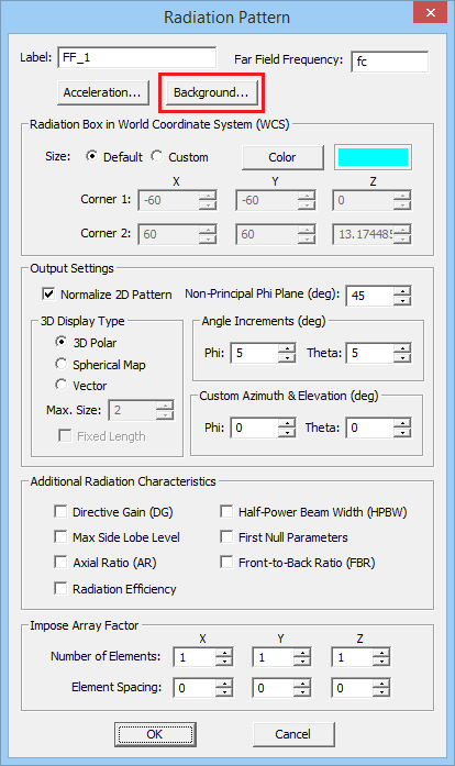
You can access these options by clicking the button labeled Background… in the Radiation Pattern dialog and opening the “Far Field Background Medium” dialog. For this project, the two options close to your structure are “PEC Ground Plane” and “Dielectric Half-Space”. However, the latter assumes a dielectric medium of infinite depth in the –Z direction, so it does not apply. A PEC ground plane is not a bad approximation as the thickness of your substrate is about 0.005 λ0. Therefore, from the radio buttons in the section titled “Set Background Medium” select the second option, i.e., PEC Ground Plane. In the section titled “Set Top Z-Coordinate”, keep the default option “Use Bottom of Domain”. This means that the infinite PEC ground plane is placed at the bottom of your computational domain, where you have already set up a PEC boundary condition.
Setting Mesh Parameters
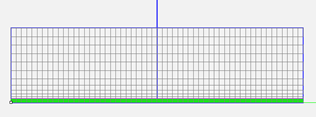
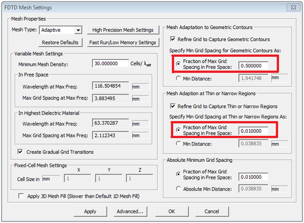
View the mesh of your structure and make sure it has good quality. Enable the YZ or ZX Grid Planes and see the side views of the structure. You will see the variable resolution in the free space and dielectric regions, as well as the gradual grid transition from the air to the dielectric substrate.
Running the FDTD Simulation & Visualizing the Results
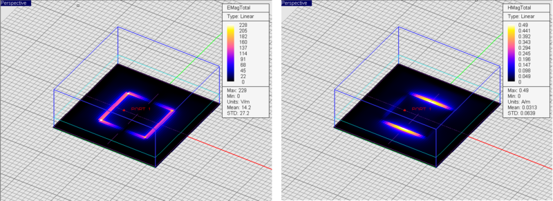
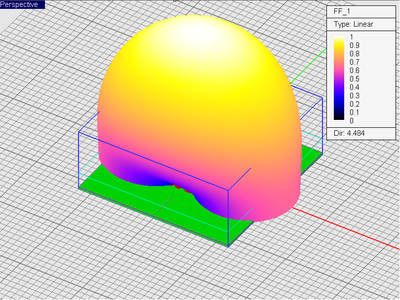
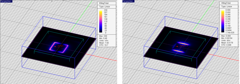
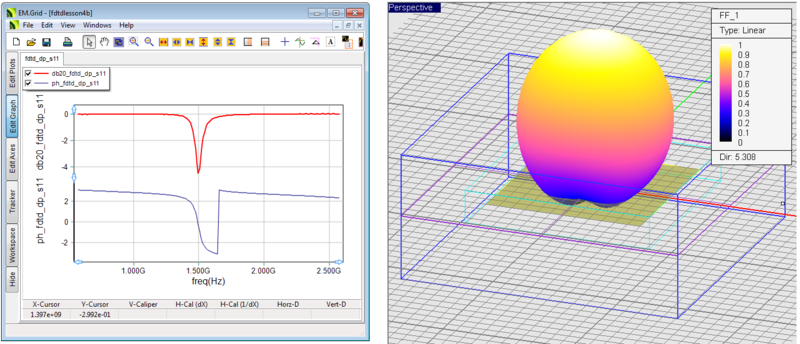
At the end of the simulation, using the Navigation Tree visualize the electric and magnetic field distributions on the patch plane as well as the 3D radiation pattern of the patch antenna. Using Data Manager, plot the S11 parameter of the probe-fed patch antenna. Note the sharp resonance of the antenna near 1.5GHz.
| |
EM.Cube’s FDTD Module does not provide a current distribution observable. However, you can define near field sensors on flat metallic plates. The tangential magnetic field components on thes senor plane represent the electric surface currents. |
Analyzing a Patch Antenna with a Finite Substrate
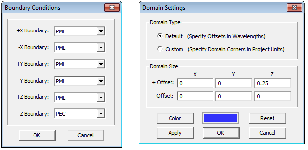
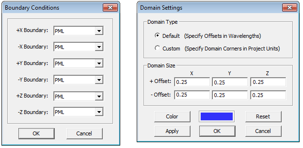
As the next step of this tutorial lesson, you will convert the dielectric substrate of your patch antenna to one with finite extents and analyze the performance of the resulting antenna. Save your project up to this point as a new project called “FDTDLesson4A”, where you will make all the new modificatios. You will use the previous part later in the next tutorial lesson. First, you are going to change the computational domain settings and its boundary conditions. Set all the boundary conditions to PML at all the six ±X, ±Y and ±Z boundaries, thus removing the previous PEC bottom boundary. Then, open the Domain Settings Dialog and restore all the six default 0.25 λ0 offsets for an open-boundary structure. You can do this very quickly by clicking the Reset button of the dialog and then clicking the Apply button. The domain walls all move away from your physical structure.
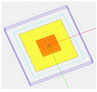
Next, realize that you new to add a new finite PEC ground to the back of your finite-sized substrate because you removed the bottom PEC boundary wall. You need to draw a new PEC rectangle strip object. First, you have to activate the PEC_1 group on the Navigation Tree. Then, draw a rectangle strip of dimensions 120mm × 120mm in a blank space and move it to the back of the dielectric box and settings its LCS coordinates to (0, 0, 0). Alternatively, hover the mouse over the bottom face of the dielectric box. The mouse cursor snaps to a small highlighted “ball” at the center of box’s bottom face. Start drawing the rectangle right from this point. Drag the mouse to snap to one of the four corners of the dielectric box and release the mouse. You get the right rectangular obejct at the right location and with the right dimensions.
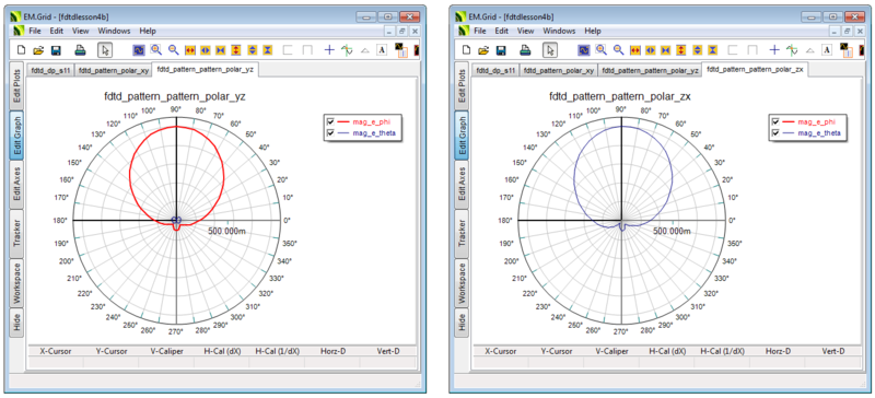
Before running a new simulation, make sure to change the settings of “Far Field Background Medium” dialog. Open the radiation pattern dialog and click the button labeled Background… In the scetion titled “Set Background Medium”, select the Free Space radio button. Now, run a quick FDTD anslysis of your new patch antenna with the finite substrate and visualize the electric and magnetic field distributions and the 3D radiation pattern. Also, plot the S11 parameter of the probe-fed patch antenna in EM.Grid as well as its 2D polar radiation pattern graphs in YZ and ZX planes.
Comparing the results of the patch antenna with the finite substrate to the one with an infinite substrate, you notice that the near field distributions are almost identical. However, the far field radiation patterns are completely different. In the finite substrate case, the radiation pattern takes a more circular shape and back lobes start to appear in the lower half-space corresponding to 0 ≤ θ ≤ 90o. Also, note that the resonant frequency of the antenna stays the same, although the S11 dip is now a little bit deeper. Moreover, in the YZ Plane, you have a large Eφ component and a very small Eθ component; while in the ZX Plane, the situation is just the opposite, with a large Eθ component and almost no Eφ component.


