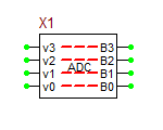
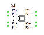
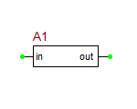
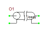
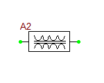
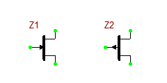
4-Bit ADC Bridge
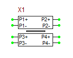
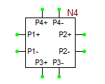
This 8-pin device is simply a bundle of 4 1-bit ADC bridges. Each analog input pin has a corresponding digital output pin.
Parameters:
| NAME | PARAMETER | UNIT | DEFAULT | NOTES |
|---|---|---|---|---|
| in_low | maximum 0-valued analog input | V | 0.1 | required |
| in_high | minimum 1-valued analog input | V | 0.9 | required |
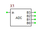
4-Bit A/D Converter Block
This is a 5-pin mixed-signal device with an analog input and 4 digital outputs. Based on the specified maximum input voltage level, a total of 16 discrete voltage levels are established. The block fits the input analog voltage between two of these 16 discrete levels and outputs the 4-bit binary equivalent to 4 digital pins B0-B3 representing the LSB and MSB, respectively.
Parameters:
| NAME | PARAMETER | UNITS | DEFAULT | NOTES |
|---|---|---|---|---|
| max_val | maximum input voltage | V | 5 |
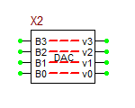
4-Bit DAC Bridge
This 8-pin device is simply a bundle of 4 1-bit DAC bridges. Each digital input pin has a corresponding analog output pin.
Parameters:
| NAME | PARAMETER | UNIT | DEFAULT | NOTES |
|---|---|---|---|---|
| out_low | analog output for 0 digital input | V | 0 | required |
| out_high | analog output for 1 digital input | V | 1 | required |
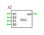
4-Bit D/A Converter Block
This is a 5-pin mixed-signal device with 4 digital inputs and an analog output. Based on the specified low and high output voltage levels, a total of 16 discrete voltage levels are established. The block converts the input 4-bit word (B0-B3 representing the LSB and MSB, respectively) to the corresponding discrete voltage level and outputs it as an analog voltage signal.
Parameters:
| NAME | PARAMETER | UNITS | DEFAULT | NOTES |
|---|---|---|---|---|
| out_low | output low voltage level | V | 0 | |
| out_high | output high voltage level | V | 5 |
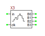
4-Bit Signal Digitizer Block
This is a 6-pin mixed-signal device with an analog input, a digital clock and 4 digital outputs. It samples its analog input signal at the period of the supplied digital clock. The digitized version of the input signal is sent out to 4 digital outputs B0-B3 representing the LSB and MSB, respectively.
Parameters:
| NAME | PARAMETER | UNITS | DEFAULT | NOTES |
|---|---|---|---|---|
| r_in | input resistance | Ω | 10G | |
| max_val | maximum input voltage | V | 5 |
50-Ohm Load
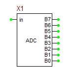
8-Bit A/D Converter Block
This is a 9-pin mixed-signal device with an analog input and 8 digital outputs. Based on the specified maximum input voltage level, a total of 256 discrete voltage levels are established. The block fits the input analog voltage between two of these 256 discrete levels and outputs the 8-bit binary equivalent to 8 digital pins B0-B7 representing the LSB and MSB, respectively.
Parameters:
| NAME | PARAMETER | UNITS | DEFAULT | NOTES |
|---|---|---|---|---|
| max_val | maximum input voltage | V | 5 |
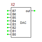
8-Bit D/A Converter Block
This is a 9-pin mixed-signal device with 8 digital inputs and an analog output. Based on the specified low and high output voltage levels, a total of 256 discrete voltage levels are established. The block converts the input 8-bit word (B0-B7 representing the LSB and MSB, respectively) to the corresponding discrete voltage level and outputs it as an analog voltage signal.
Parameters:
| NAME | PARAMETER | UNITS | DEFAULT | NOTES |
|---|---|---|---|---|
| out_low | output low voltage level | V | 0 | |
| out_high | output high voltage level | V | 5 |
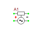
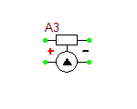
AC/RF Current Source
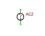
This is a simplified version of the standard Current Source, in which the AC "Use" box has been checked by default. Therefore, it is ready to be used for AC frequency sweep. Note that for AC frequency sweep, you do not need to specify the frequency.
Parameters:
| NAME | PARAMETER | UNIT | DEFAULT | NOTES |
|---|---|---|---|---|
| VA | peak current amplitude | A | 1 | required |
| Freq | frequency | Hz | 1 | required |
| Phase | phase | deg | 0 | |
| offset | DC offset for small-signal current | A | 0 |
AC/RF Voltage Source
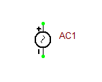
This is a simplified version of the standard Voltage Source, in which the AC "Use" box has been checked by default. Therefore, it is ready to be used for AC frequency sweep. Note that for AC frequency sweep, you do not need to specify the frequency.
Parameters:
| NAME | PARAMETER | UNIT | DEFAULT | NOTES |
|---|---|---|---|---|
| VA | peak voltage amplitude | V | 1 | required |
| Freq | frequency | Hz | 1 | required |
| Phase | phase | deg | 0 | |
| offset | DC offset for small-signal voltage | V | 0 |
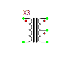
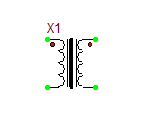
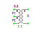
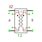
Alternate Ferrite Core Transformer
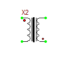
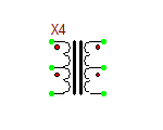
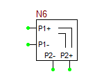
The alternate ferrite core transformer is a four-pin two-port device, which has the same behavior as the Ferrite Core Transformer, except for the reversed polarity of its secondary port.
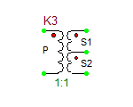
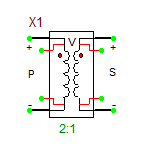
Alternate Ideal Transformer
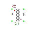
The alternate ideal transformer is a four-pin two-port device, which has the same behavior as the Ideal Transformer, except for the reversed polarity of its secondary port.
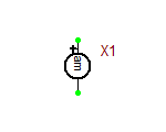
AM Modulated Source
This is a voltage source with a single-tone amplitude modulated waveform. The AM modulation index MDI is defined as the ratio of maximum amplitude deviation to maximum signal amplitude.
Parameters:
| NAME | PARAMETER | UNIT | DEFAULT | NOTES |
|---|---|---|---|---|
| V0 | offset | V | 0 | |
| VA | amplitude | V | 1 | |
| FC | carrier frequency | Hz | 1 | required |
| MDI | modulation index | - | 0 | required |
| FS | signal frequency | Hz | 1 | required |
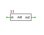
Amplitude Modulator Block
This device takes an input signal and generates an AM modulated output signal of a specified carrier frequency with a specified modulation index.
Parameters:
| NAME | PARAMETER | UNITS | DEFAULT | NOTES |
|---|---|---|---|---|
| r_in | input resistance | Ω | 1G | |
| r_out | output resistance | Ω | 1u | |
| m | modulation index | - | 0.5 | |
| fc | carrier frequency | Hz | 1Meg | |
| ac | carrier peak amplitude | V | 1 |
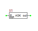
Amplitude Shift-Keying Modulator Block
This device takes a digital input like a binary sequence and generates an ASK modulated output signal with two specified carrier amplitude levels.
Parameters:
| NAME | PARAMETER | UNITS | DEFAULT | NOTES |
|---|---|---|---|---|
| r_out | output resistance | Ω | 1u | |
| fc | carrier frequency | Hz | 1Meg | |
| ac_lo | low carrier peak amplitude | V | 0.0 | |
| ac_hi | high carrier peak amplitude | V | 1.0 |
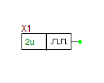
Analog Clock
This is a periodic pulse generator with a default 0V low output level and a default 5V high output level.
Parameters:
| NAME | PARAMETER | UNIT | DEFAULT | NOTES |
|---|---|---|---|---|
| delay | delay time | sec | 0 | |
| rise | rise time | sec | 0.1n | |
| fall | fall time | sec | 0.1n | |
| pulse_wid | clock pulse width | sec | 1u | required |
| period | clock period | - | 2u | required |
| out_low | low output voltage level | V | 0 | |
| out_high | high output voltage level | V | 5 |
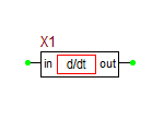
Analog Differentiator Block
This device outputs the derivative of its input signal. It is a native RF.Spice A/D block and different from the XSPICE Differentiator Block, which is a more extensive model.
Parameters:
| NAME | PARAMETER | UNITS | DEFAULT | NOTES |
|---|---|---|---|---|
| gain | gain | - | 1.0 | |
| offset | offset voltage | V | 0 | |
| fmax | maximum signal frequency | Hz | 1Meg |
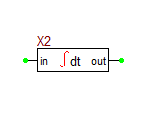
Analog integrator Block
This device outputs the integral of its input signal assuming zero initial conditions. It is a native RF.Spice A/D block and different from the XSPICE Integrator Block, which is a more extensive model.
Parameters:
| NAME | PARAMETER | UNITS | DEFAULT | NOTES |
|---|---|---|---|---|
| gain | gain | - | 1.0 | |
| offset | offset voltage | V | 0 | |
| fmax | maximum signal frequency | Hz | 1Meg |
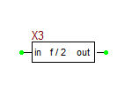
Analog One-Half Frequency Divider Block
This device takes a harmonic input signal and generates a harmonic output signal with a frequency one half lower and a user specified amplitude.
Parameters:
| NAME | PARAMETER | UNITS | DEFAULT | NOTES |
|---|---|---|---|---|
| r_in | input resistance | Ω | 1G | |
| r_out | output resistance | Ω | 1u | |
| max_val | output amplitude | V | 1.0 |
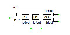
Analog Phase-Locked Loop Block
This 5-pin device is a parameterized model of an analog phase-locked loop. It provides two phase-locked output signals with square wave and triangular wave waveforms. The outputs of the lowpass filter and phase detector are also accessible via the designated pins.
Parameters:
| NAME | PARAMETER | UNITS | DEFAULT | NOTES |
|---|---|---|---|---|
| r_in | input resistance | Ω | 1G | |
| r_out | output resistance | Ω | 1u | |
| K_d | voltage conversion factor of phase detector | V/rad | 1.0 | |
| K_f | frequency conversion factor of VCO | Hz/V | 1k | |
| V_sq | square wave output peak amplitude | V | 1 | |
| V_tri | triangular wave output peak amplitude | V | 1 | |
| VT | VCO input dynamic range | V | 1 | |
| r_time | VCO timing resistor | Ω | 12k | |
| c_time | VCO timing capacitor | F | 10n | |
| fo | VCO free-running frequency | Hz | 1k | |
| r_lpf | lowpass filter resistor | Ω | 10k | |
| c_lpf | lowpass filter capacitor | F | 100n |
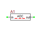
Analog-to-Digital Converter (ADC) Bridge
The ADC Bridge takes an analog value from an analog node and may be in the form of a voltage or current. If the input is less than or equal to "in_low", then a digital "0" is generated. If the input is greater than or equal to "in_high", a digital "1" is generated. Otherwise, a digital "UNKNOWN" is the output value. Unlike the DAC Bridge, ramping or delay is not applicable. Rather, the continuous ramping of the input provides for any associated delays in the digitized signal.
This model also posts an input load value based on the parameter input_load.
Model Identifier: adc_bridge
Netlist Format:
A<device_name> [<in_pin> {<in2_pin>> ...}] [<out_pin> {<out2_pin> ...}] <model_name>
.model <model_name> adc_bridge {<param1 = value> < param2 = value> ...}
Example:
A [1] [2] adc_bridge
.model adc_bridge adc_bridge in_low = .1 fall_delay = 1n
Parameters:
| NAME | PARAMETER | UNIT | DEFAULT | NOTES |
|---|---|---|---|---|
| in_low | maximum 0-valued analog input | V | 0.1 | required |
| in_high | minimum 1-valued analog input | V | 0.9 | required |
| rise_delay | L-to-H delay time | sec | 1n | |
| fall_delay | H-to-L delay time | sec | 1n |
Arbitrary Temporal Waveform Generator
This is a voltage source with an arbitrary waveform defined by a mathematical expression. You have to open the subcircuit model dialog by clicking the View Subcircuit button and edit its text. Enter any mathematical expression in the variable "v(t)" standing for time.
Examples:
- v(t) is equivalent to f(t) = t.
- 0.1*(v(t))^2 is equivalent to f(t) = 0.1t^2.
- sin(2*pi*v(t)) is equivalent to f(t) = sin(2Ït).
Parameters:
| NAME | PARAMETER | UNIT | DEFAULT | NOTES |
|---|---|---|---|---|
| Tmax | maximum signal duration | sec | 1e6 | required |
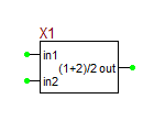
Arithmetic Mean Block
This 3-pin device sends the arithmetic mean or average of its two inputs to the output with a default unity gain.
Parameters:
| NAME | PARAMETER | UNITS | DEFAULT | NOTES |
|---|---|---|---|---|
| gain | gain | - | 1.0 |
Attenuator: Pi-Type
This is a four-pin, two-port device that models a resistive power attenuator with the "Pi" configuration. The characteristic impedances of the input and output transmission lines can be different. The K-parameter is the power attenuation ratio from the input to the output.
Model Identifier: attenuator Pi Bold text
Parameters:
| NAME | PARAMETER | UNITS | DEFAULT | NOTES |
|---|---|---|---|---|
| Zo1 | input line characteristic impedance | Ohms | 50.0 | |
| Zo2 | output line characteristic impedance | Ohms | 50.0 | |
| K | input/output power ratio | - | 1.0 |
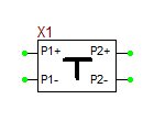
Attenuator: T-Type
This is a four-pin, two-port device that models a resistive power attenuator with the "T" configuration. The characteristic impedances of the input and output transmission lines can be different. The K-parameter is the power attenuation ratio from the input to the output.
Model Identifier: attenuator T
Parameters:
| NAME | PARAMETER | UNITS | DEFAULT | NOTES |
|---|---|---|---|---|
| Zo1 | input line characteristic impedance | Ohms | 50.0 | |
| Zo2 | output line characteristic impedance | Ohms | 50.0 | |
| K | input/output power ratio | - | 1.0 |
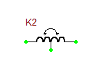
Auto-Transformer
This 3-pin device models an auto-transformer with mutual coupling effect.
Parameters:
| NAME | PARAMETER | UNIT | DEFAULT | NOTES |
|---|---|---|---|---|
| Lp | primary inductance | H | 1m | |
| Ls | secondary inductance | H | 1m | |
| k | coefficient of coupling | - | 1.0 |
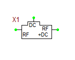
Bias Tee
This is a six-pin, three-port device that models a passive RF bias tee. The two RF and DC inputs mix into the output (RF+DC) port.
Model Identifier: bias-tee
Parameters:
| NAME | PARAMETER | UNITS | DEFAULT | NOTES |
|---|---|---|---|---|
| L | inductance | nH | 100.0 | |
| C | capacitance | nF | 100.0 |
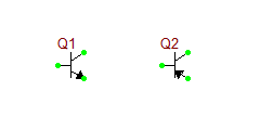
Bipolar Junction Transistor (BJT)
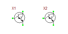
The BJT is an active device which has up to 4 pins. The three standard pins are base, emitter, and collector. These are given in the default symbol. The substrate, which is grounded by default, is the fourth pin. To use the BJT with the substrate, create a new 4-pin BJT using the Device Editor and Symbol Editor.
The standard device parameters are AREA, OFF, IC, and T. They are described below:
| AREA | area factor (optional) (If not specified, the default value is 1.0.) |
| OFF | initial condition for the DC analysis (optional) |
| IC | initial condition (optional) (Used when a transient analysis is desired, which starts from other than the quiescent operating point.) |
| T | operating temperature of the device (optional) |
Area factor scales the model parameters RE and RC. IC VBE is the initial voltage from base emitter. IC VCE is the initial voltage from collector to emitter. TEMP is the overriding temperature. These parameters are based on the Gummel and Poon integral-charge model. If these parameters are not specified, then it will reduce to the simpler Ebers-Moll model.
The process model is mandatory for the BJT. Descriptions of the process model parameters are given in the following table:
| NAME | PARAMETER | UNITS | DEFAULT | EXAMPLE |
|---|---|---|---|---|
| IS | transport saturation current | A | 1.0e-16 | 1.0e-15 |
| BF | ideal maximum forward beta | 100 | 100 | |
| NF | forward current emission coefficient | 1.0 | 1 | |
| VAF | forward Early voltage | V | infinite | 200 |
| IKF | corner forward beta high current roll-off | A | infinite | 0.01 |
| ISE | B-E leakage saturation current | A | 0 | 1.0e-13 |
| NE | B-E leakage emission coefficient | 1.5 | 2 | |
| BR | ideal maximum reverse beta | 1 | 0.1 | |
| NR | reverse current emission coefficient | 1 | 1 | |
| VAR | reverse Early voltage | V | infinite | 200 |
| IKR | corner reverse beta high current roll-off | A | infinite | 0.01 |
| ISC | B-C leakage saturation current | A | 0 | 1.0e-13 |
| NC | B-C leakage emission coefficient | 2 | 1.5 | |
| RB | zero bias base resistance | ohms | 0 | 100 |
| IRB | current where base resistance falls halfway to minimum value | A | infinite | 0.1 |
| RBM | minimum base resistance at high currents | ohms | RB | 10 |
| RE | emitter resistance | ohms | 0 | 1 |
| RC | collector resistance | ohms | 0 | 10 |
| CJE | B-E zero bias depletion capacitance | F | 0 | 2pF |
| VJE | B-E built-in potential | V | 0.75 | 0.6 |
| MJE | B-E junction exponential factor | 0.33 | 0.33 | |
| TF | ideal forward transit time | sec | 0 | 0.1ns |
| XTF | coefficient for bias dependence of TF | 0 | ||
| VTF | voltage describing VBC dependence of TF | V | infinite | |
| ITF | high-current parameter for effect on TF | A | 0 | |
| PTF | excess phase at freq=1.0/(TF*2PI)Hz | degree | 0 | |
| CJC | B-C zero bias depletion capacitance | F | 0 | 2pF |
| VJC | B-C built-in potential | V | 0.75 | 0.5 |
| MJC | B-C junction exponential factor | 0.33 | 0.5 | |
| XCJC | fraction of B-C depletion capacitance connected to internal base node | 1 | ||
| TR | ideal reverse transit time | sec | 0 | 10ns |
| CJS | zero bias collector-substrate capacitance | F | 0 | 2pF |
| VJS | substrate junction built-in potential | V | 0.75 | |
| MJS | substrate junction exponential factor | 0 | 0.5 | |
| XTB | forward and reverse beta temp. exponent | 0 | ||
| EG | energy gap for temperature effect on IS | eV | 1.11 | |
| XTI | temperature exponent for effect on IS | 3 | ||
| KF | flicker-noise coefficient | 0 | ||
| AF | flicker-noise exponent | 1 | ||
| FC | coefficient for forward bias depletion capacitance formula | 0.5 | ||
| TNOM | parameter measurement temperature | deg. C | 27 | 50 |
Bond Wire Above Ground
This is a two-pin, one-port device that models a bond wire including the ground effect.
Model Identifier: BondWire-Free
Parameters:
| NAME | PARAMETER | UNITS | DEFAULT | NOTES |
|---|---|---|---|---|
| r | wire radius | mm | 0.1 | |
| l | pad spacing | mm | 1.0 | |
| h | height above ground | mm | 1.0 | |
| sigma | wire conductivity | S/m | 1e8 |
Bond Wire (Free-Space)
This is a two-pin, one-port device that models a bond wire with no ground effect.
Model Identifier: BondWire-Free
Parameters:
| NAME | PARAMETER | UNITS | DEFAULT | NOTES |
|---|---|---|---|---|
| r | wire radius | mm | 0.1 | |
| l | pad spacing | mm | 1.0 | |
| sigma | wire conductivity | S/m | 1e8 |
Branchline Hybrid Coupler
This is an eight-pin, four-port device that models a branchline quadrature hybrid coupler. If Port 1 acts as an input port, the output power is equally split between Ports 2 and 3. Port 2 has 90° phase shift with respect to the input, while Port 3 is in-phase with respect to the input. Port 4 acts as an isolated port. Since the branchline hybrid has a symmetric structure, any port can serve as the input port. You have to specify the center frequency of the device in GHz.
Model Identifier: branchline
Parameters:
| NAME | PARAMETER | UNITS | DEFAULT | NOTES |
|---|---|---|---|---|
| Z0 | line characteristic impedance | Ohms | 50.0 | |
| eeff | effective permittivity | - | 1.0 | |
| fc | center frequency | GHz | 1.0 | |
| len | port line segment length | mm | 10.0 |
Capacitance Meter
The Capacitance Meter measures the total capacitance between a circuit node and the ground. The input pin of the device is connected to the measurement node. The output voltage of the device is then a scaled value equal to the total capacitance seen on its input multiplied by the gain parameter. This model is primarily intended as a building block for other models which must sense a capacitance value and alter their behavior based upon it.
Model Identifier: cmeter
Netlist Format:
A<device_name> <in_pin> <out_pin> <model_name>
.model <model_name> cmeter {<gain = value>}
Example:
A1 1 2 cap_meter
.model cap_meter cmeter gain = 1
Parameters:
The only parameter is the gain with a default value of 1.0.
Capacitor
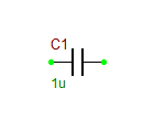
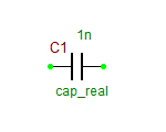
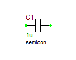
Capacitors are used to store electrical energy. They can filter or remove AC signals or block DC current without disrupting AC signals. A capacitor's ability to store energy is termed capacitance and is measured in Farads, with values from pF to mF. The only time current flows through a capacitor is when the charge is collected on, or is removed from, its parallel plates. This means that the voltage across the capacitor is changing, which doesn't conform to DC analysis. In a physical circuit, there is a transition stage during which capacitors charge up to their final values. The result is the same as if these capacitors did not exist and the connections to them were left dangling. In other words, in a (steady-state) DC analysis, a capacitor behaves like an open circuit. Therefore, it is important that no section of the circuit is isolated from the capacitors. Every circuit node needs some path for DC current to the ground.
A capacitor's transient behavior is described by the equation:
i(t) = C * (dv(t)/dt)
Its initial voltage is only important when the simulator performs a transient analysis, and the "Use Initial Conditions" checkbox is checked.
An capacitor's AC behavior is described by the equation:
i = j Ï * C * v
All capacitor names must begin with C.
Netlist Format:
C<device_name> <N+> <N-> <value>
Example:
C1 1 2 10p
RF.Spice A/D provides three types of capacitors: simple, user-defined (or real) and semiconductor. The standard capacitor parameters are N+, N-, VALUE, and IC. In a simple capacitor, VALUE must be specified for the capacitance in Farads. IC is the (optional) initial condition for the capacitor voltage.
Center-Tapped Ferrite Core Transformer
This five-pin three-port device models a center-tapped physical transformer with a magnetic ferrite core. Its model is based on XSPICE's magnetic core and inductive coupling models. For this device you need to specify physical parameters like cross sectional area, core length and number of primary and secondary turns. The physical model of the magnetic device is defined by two vectors: magnetic field intensity H in A/m and magnetic flux density B (also known as magnetic induction) in Tesla. The default array values are:
H_array = [-250 -100 -50 -37.5 -25 -12.5 0 12.5 25 37.5 50 100 250]
B_array = [-0.375 -0.36 -0.32 -0.29 -0.24 -0.15 0 0.15 0.24 0.29 0.32 0.36 0.375]
To change the value of H/B arrays, open the subcircuit model dialog by clicking the View Subcircuit button and edit its text.
Parameters:
| NAME | PARAMETER | UNITS | DEFAULT | NOTES |
|---|---|---|---|---|
| n_prim | number of primary inductor coupling turns | - | 100 | required |
| n_sec | number of full-winding secondary inductor coupling turns | - | 100 | required |
| area | cross-sectional area | m2 | 1e-5 | |
| length | core length | m | 0.01 |
Chip Resistor
This is a four-pin, two-port device that models a semiconductor chip resistor. The resistor is made of a thin film deposited between two Ohmic pads on a dielectric substrate.
Model Identifier: chip resistor
Parameters:
| NAME | PARAMETER | UNITS | DEFAULT | NOTES |
|---|---|---|---|---|
| w | thin film width | mm | 1.0 | |
| l | thin film length | mm | 2.0 | |
| d | thin film thickness | mm | 0.1 | |
| sigma | thin film conductivity | S/m | 5.0 | |
| wp | Ohmic pad width | mm | 2.0 | |
| h | substrate thickness | mm | 1.6 | |
| er | substrate relative permittivity | - | 2.2 |
Clocked Sample-and-Hold Block
This device samples its input signal at a specified sampling period and holds the values of each sample during each clock cycle. The output signal is a quantized version of the input signal.
Parameters:
| NAME | PARAMETER | UNITS | DEFAULT | NOTES |
|---|---|---|---|---|
| T | sampling period | sec | 1 | required |
| duty_cycle | sampling pulse duty cycle | - | 0.1 | |
| Tmax | signal period or maximum duration | sec | 10 |
Coaxial Line
This is a four-pin, two-port device that models a coaxial line segment with a dielectric core.
Model Identifier: coaxial-line
Parameters:
| NAME | PARAMETER | UNITS | DEFAULT | NOTES |
|---|---|---|---|---|
| r_in | inner conductor radius | mm | 5.0 | |
| r_out | outer conductor radius | mm | 10.0 | |
| er | core dielectric relative permittivity | - | 2.2 | |
| len | coaxial line length | mm | 10.0 | |
| sigma | metal conductivity | S/m | 1e10 | |
| tand | core dielectric loss tangent | - | 0 |
Coaxial Step in Inner Conductor
This is a four-pin, two-port device that models a step in inner conductor radius between two coaxial lines of equal outer conductor radius with a dielectric core.
Model Identifier: coaxial-innerstep
Parameters:
| NAME | PARAMETER | UNITS | DEFAULT | NOTES |
|---|---|---|---|---|
| r_in1 | smaller inner conductor radius | mm | 2.0 | |
| r_in2 | larger inner conductor radius | mm | 4.0 | |
| r_out | outer conductor radius | mm | 5.0 | |
| er | core dielectric relative permittivity | - | 2.2 |
Coaxial Step in Outer Conductor
This is a four-pin, two-port device that models a step in outer conductor radius between two coaxial lines of equal inner conductor radius with a dielectric core.
Model Identifier: coaxial-outerstep
Parameters:
| NAME | PARAMETER | UNITS | DEFAULT | NOTES |
|---|---|---|---|---|
| r_in | inner conductor radius | mm | 2.0 | |
| r_out1 | smaller outer conductor radius | mm | 4.0 | |
| r_out2 | larger outer conductor radius | mm | 6.0 | |
| er | core dielectric relative permittivity | - | 2.2 |
Comparator with Hysteresis
This device is a 3-pin two-signal voltage comparator block with hysteresis effect. If the output voltage is at its low level and you increase Îv = (vpos - vneg), the output switches to the high level as soon as Îv > V_hys. If the output voltage is at its high level and you decrease Îv = (vpos - vneg), the output switches to the low level as soon as Îv < -V_hys.
Parameters:
| NAME | PARAMETER | UNITS | DEFAULT | NOTES |
|---|---|---|---|---|
| V_hi | high output voltage level | V | 5 | |
| V_lo | high output voltage level | v | 100m | |
| V_hys | hysteresis voltage width | V | 50m |
Complex Impedance
This is a two-pin, one-port device that models a generic impedance with both real and imaginary parts. It can be used in place of a one-port device when input impedance data are available rather than s11-parameter values.
Model Identifier: impedance
Parameters:
A table of z11-parameter values as a function of frequency
Complex Modulus Block
This 3-pin device assumes its first and second input signals to be the real and imaginary parts of a complex signal and sends the absolute value of such a complex signal to the output with a default unity gain.
Parameters:
| NAME | PARAMETER | UNITS | DEFAULT | NOTES |
|---|---|---|---|---|
| gain | gain | - | 1.0 |
Conductor-Backed CPW Line
This is a four-pin, two-port device that models a conductor-backed coplanar waveguide (CPW) line segment on a single-layer dielectric substrate with a ground plane.
Model Identifier: cbcpw-line
Parameters:
| NAME | PARAMETER | UNITS | DEFAULT | NOTES |
|---|---|---|---|---|
| w | slot width | mm | 2.0 | |
| s | center strip width | mm | 2.0 | |
| h | substrate thickness | mm | 1.6 | |
| er | substrate relative permittivity | - | 2.2 | |
| len | cpw line length | mm | 10.0 |
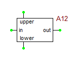
Controlled Limiter Block
The Controlled Limiter is a single-input, single-output block similar to the Gain Block. However, the output of the Controlled Limiter function is restricted to the range specified by the output lower and upper limits. This model operates in DC, AC and Transient analysis modes. Note that the limit range is the value below the Upper Limit Control input signal (CNTL_UPPER) and above the Lower Limit Control input signal (CNTL_LOWER) at which smoothing of the output signal begins. A minimum positive value of voltage difference must exist between the CNTL_UPPER and CNTL_LOWER inputs at all times. The main difference between the Controlled Limiter Block and the Limiter Block is that the former's limits are set by input control voltages, while the latter's limits are set as numerical parameters.
Also note that the Controlled Limiter function examines the input values of CNTL_UPPER and CNTL_LOWER to make sure that they are spaced far enough apart to guarantee the existence of a linear range between them. The range is calculated as the difference between (cntl_upper - upper_delta - limit_range) and (cntl_lower + lower_delta + limit_range) and must be greater than or equal to zero. When the limit_range is specified as a fractional value, the limit_range used in the above is taken as the calculated fraction of the difference between cntl_upper and cntl_lower. Still, the potential exists for too great a limit_range value to be specified for proper operation, in which case the model will return an error message.
Model Identifier: climit
Netlist Format:
A<device_name> <in_pin> <cntl_upper_pin> <cntl_lower_pin> <out_pin> <model_name>
.model <model_name> climit {<param1 = value> < param2 = value> ...}
Example:
A1 1 2 3 4 controlled_limit_block
.model controlled_limit_block climit in_offset = 0.0 gain = 1.0 upper_delta = 0.0 lower_delta = 0.0
Parameters:
| NAME | PARAMETER | UNITS | DEFAULT | NOTES |
|---|---|---|---|---|
| in_offset | input offset | V | 0.0 | |
| gain | gain | - | 1.0 | |
| upper_delta | output upper delta | - | 0.0 | |
| lower_delta | output lower delta | - | 0.0 | |
| limit_range | upper and lower sm. Range | - | 1.0e-6 | |
| fraction | smoothing %/abs switch | - | False |
Controlled One-Shot
This is an eight-terminal function generator with a single pulse output. The pulse width is controlled by an input voltage. The functional dependency of the output pulse width on the input voltage is piecewise linear and is defined as a two-dimensional table similar to a piecewise linear (PWL) controlled source. In the "pulse width vs. voltage" curve, the array "cntl_array" defines voltage values in Volts and the array "pw_array" defines the corresponding pulse width values in seconds.
The generation of the output pulse is triggered either on the rising or falling edge of a clock input.
Model Identifier: oneshot
Netlist Format:
A<device_name>Â %vd(<clk_pin> <clk_ref_pin>)Â %vd(<cntl_in_pin> <cntl_in_ref_pin>) %vd(<clear_pin> <clear_ref_pin>) %vd(<out_pin> <out_ref_pin>) <model_name>
.model <model_name> oneshot {<param1 = value> < param2 = value> ...}
Example:
A1Â %vd(1 5) Â %vd(2 6) Â %vd(3 7) Â %vd(4 8) one_shot
.model one_shot oneshot cntl_array = [0.0] pw_array = [1u] rise_time = 1n
Parameters:
| NAME | PARAMETER | UNIT | DEFAULT | NOTES |
|---|---|---|---|---|
| Clk_trig | clock trigger value | V | 0.5 | |
| Pos_edge_trig | positive/negative edge trigger switch | - | True | |
| Cntl_array | control array | V | [0.0] | required |
| Pw_array | pulse width array | sec | [1u] | required |
| Out_low | output low value | V | 0.0 | |
| Out_high | output high value | V | 1.0 | |
| Delay | output delay from trigger | sec | 1.0e-9 | |
| Rise_time | output rise time | sec | 1.0e-9 | |
| Fall_time | output fall time | sec | 1.0e-9 |
Controlled Sine Wave Oscillator
This is a four-terminal function generator with a sinusoidal wave output, whose frequency is controlled by an input voltage. The functional dependency of the output frequency on the input voltage is piecewise linear and is defined as a two-dimensional table similar to a piecewise linear (PWL) controlled source. In the "frequency vs. voltage" curve, the array "cntl_array" defines voltage values in Volts and the array "freq_array" defines the corresponding frequencies in Hz. This function has parameterizable values of low and high peak output voltage.
Model Identifier: sine
Netlist Form:
A<device_name>Â %vd(<cntl_in_pin> <cntl_in_ref_pin>)Â %vd(<out_pin> <out_ref_pin>) <model_name>
.model <model_name> sine cntl_array = [<value1> <value2>] freq_array = [<value1> <value2>] {<param1 = value> < param2 = value> ...}
Example:
A1Â %vd(1 3) Â %vd(2 4) sine
.model sine sine cntl_array = [0 1] freq_array = [1 1000]
Parameters:
| NAME | PARAMETER | UNIT | DEFAULT | NOTES |
|---|---|---|---|---|
| Cntl_array | control array | V | [0 1] | required |
| Freq_array | frequency array | Hz | [1 1000] | required |
| Out_low | output peak low value | V | -1.0 | |
| Out_high | output peak high value | V | 1.0 |
Controlled Sources
Circuits can contain linear dependent sources characterized by one of the following equations (where g, e, f, and h are constants representing transconductance, voltage gain, current gain, and transresistance, respectively):
iout = g vin      vout = e vin      iout = f iin      vout = h iin
For further information, refer to:
Linear Current Controlled Current Source (CCCS)
Linear Voltage Controlled Current Source (VCCS)
Linear Current Controlled Voltage Source (CCVS)
Linear Voltage Controlled Voltage Source (VCVS)
Controlled Square Wave Oscillator
This is a four-terminal function generator with a square wave output, whose frequency is controlled by an input voltage. The functional dependency of the output frequency on the input voltage is piecewise linear and is defined as a two-dimensional table similar to a piecewise linear (PWL) controlled source. In the "frequency vs. voltage" curve, the array "cntl_array" defines voltage values in Volts and the array "freq_array" defines the corresponding frequencies in Hz.
Model Identifier: square
Netlist Format:
A<device_name>Â %vd(<cntl_in_pin> <cntl_in_ref_pin>)Â %vd(<out_pin> <out_ref_pin>) <model_name>
.model <model_name> square cntl_array = [<value1> <value2>] freq_array = [<value1> <value2>] {<param1 = value> < param2 = value> ...}
Example:
A1Â %vd(1 3) Â %vd(2 4) square
.model square square cntl_array = [0 1] freq_array = [1 1000]
Parameters:
| NAME | PARAMETER | UNIT | DEFAULT | NOTES |
|---|---|---|---|---|
| Cntl_array | control array | V | [0 1] | required |
| Freq_array | frequency array | Hz | [0 1000] | required |
| Out_low | output peak low value | V | -1.0 | |
| Out_high | output peak high value | V | 1.0 | |
| Duty_cycle | Duty cycle | - | 0.5 | |
| Rise_time | Output rise time | sec | 1.0e-9 | |
| Fall_time | Output fall time | sec | 1.0e-9 |
Controlled Triangle Wave Oscillator
This is a four-terminal function generator with a triangle wave output, whose frequency is controlled by an input voltage. The functional dependency of the output frequency on the input voltage is piecewise linear and is defined as a two-dimensional table similar to a piecewise linear (PWL) controlled source. In the "frequency vs. voltage" curve, the array "cntl_array" defined voltage values in Volts and the array "freq_array" defines the corresponding frequencies in Hz.
Model Identifier: triangle
Netlist Format:
A<device_name>Â %vd(<cntl_in_pin> <cntl_in_ref_pin>)Â %vd(<out_pin> <out_ref_pin>) <model_name>
.model <model_name> tirangle cntl_array = [<value1> <value2>] freq_array = [<value1> <value2>]{<param1 = value> < param2 = value> ...}
Example:
A1Â %vd(1 4) Â %vd(2 3) triangle
.model triangle triangle cntl_array = [0 1] freq_array = [1 1000]
Parameters:
| NAME | PARAMETER | UNIT | DEFAULT | NOTES |
|---|---|---|---|---|
| Cntl_array | control array | V | [0 1] | required |
| Freq_array | frequency array | Hz | [0 1000] | required |
| Out_low | output peak low value | V | -1.0 | |
| Out_high | output peak high value | V | 1.0 | |
| Rise_duty | Rise time duty cycle | 0.5 |
Coplanar Strips (CPS) Line
This is a four-pin, two-port device that models a coplanar strips (CPS) line segment on a single-layer conductor-backed dielectric substrate.
Model Identifier: cps-line
Parameters:
| NAME | PARAMETER | UNITS | DEFAULT | NOTES |
|---|---|---|---|---|
| w | strip width | mm | 2 | |
| w | strip spacing | mm | 2 | |
| h | substrate thickness | mm | 1.6 | |
| er | substrate relative permittivity | - | 2.2 | |
| len | line segment length | m | 10 |
Coplanar Waveguide (CPW) Line
This is a four-pin, two-port device that models a coplanar waveguide (CPW) line segment on a single-layer dielectric substrate without a ground backing.
Model Identifier: cpw-line
Parameters:
| NAME | PARAMETER | UNITS | DEFAULT | NOTES |
|---|---|---|---|---|
| w | slot width | mm | 2.0 | |
| s | center strip width | mm | 2.0 | |
| h | substrate thickness | mm | 1.6 | |
| er | substrate relative permittivity | - | 2.2 | |
| len | cpw line length | mm | 10.0 | |
| sigma | metal conductivity | S/m | 1e10 | |
| tand | substrate dielectric loss tangent | - | 0 | |
| t | metallization thickness | mm | 0 |
Coupled Microstrip Lines
This is an eight-pin, four-port device that models two parallel coupled microstrip line segments on a single-layer conductor-backed dielectric substrate.
Model Identifier: coupled-microstrips
Parameters:
| NAME | PARAMETER | UNITS | DEFAULT | NOTES |
|---|---|---|---|---|
| w | microstrip width | mm | 4.8 | |
| s | microstrip spacing | mm | 5.0 | |
| h | substrate thickness | mm | 1.6 | |
| er | substrate relative permittivity | - | 2.2 | |
| len | microstrip length | mm | 10.0 |
Coupled Striplines
This is an eight-pin, four-port device that models two side-by-side parallel coupled stripline segments sandwiched between two parallel plates with a dielectric spacer. In this model, the two striplines are placed at the center of the dielectric with equal distances from the top and bottom plates.
Model Identifier: coupled-striplines
Parameters:
| NAME | PARAMETER | UNITS | DEFAULT | NOTES |
|---|---|---|---|---|
| w | microstrip width | mm | 4.8 | |
| s | microstrip spacing | mm | 5.0 | |
| b | parallel plate spacing | mm | 3.2 | |
| er | substrate relative permittivity | - | 2.2 | |
| len | stripline length | mm | 10.0 |
Covered CPW Line
This is a four-pin, two-port device that models a covered coplanar waveguide (CPW) line segment on a single-layer dielectric substrate without a ground backing but with a metal cover plate.
Model Identifier: cpw-covered
Parameters:
| NAME | PARAMETER | UNITS | DEFAULT | NOTES |
|---|---|---|---|---|
| w | slot width | mm | 2.0 | |
| s | center strip width | mm | 2.0 | |
| h | substrate thickness | mm | 1.6 | |
| er | substrate relative permittivity | - | 2.2 | |
| hc | cover height | mm | 10 | |
| len | cpw line length | mm | 10 |
Covered Conductor-Backed CPW Line
This is a four-pin, two-port device that models a covered conductor-backed coplanar waveguide (CPW) line segment on a single-layer dielectric substrate with both a ground plane and a metal cover plate.
Model Identifier: cbcpw-line
Parameters:
| NAME | PARAMETER | UNITS | DEFAULT | NOTES |
|---|---|---|---|---|
| w | slot width | mm | 2.0 | |
| s | center strip width | mm | 2.0 | |
| h | substrate thickness | mm | 1.6 | |
| er | substrate relative permittivity | - | 2.2 | |
| hc | cover height | mm | 10 | |
| len | cpw line length | mm | 10 |
Covered Microstrip Line
This is a four-pin, two-port device that models a covered microstrip line segment on a single-layer conductor-backed dielectric substrate.
Model Identifier: microstrip-covered
Parameters:
| NAME | PARAMETER | UNITS | DEFAULT | NOTES |
|---|---|---|---|---|
| w | microstrip width | mm | 4.8 | |
| h | substrate thickness | mm | 1.6 | |
| er | substrate relative permittivity | - | 2.2 | |
| h | cover height | mm | 10 | |
| len | microstrip length | m | 10 |
CPW Gap
This is a four-pin, two-port device that models a gap-in-width transition between two coplanar waveguide (CPW) lines on a single-layer dielectric substrate without a ground backing.
Model Identifier: cpw-gap
Parameters:
| NAME | PARAMETER | UNITS | DEFAULT | NOTES |
|---|---|---|---|---|
| w | slot width | mm | 2.0 | |
| s | center strip width | mm | 2.0 | |
| g | center strip gap spacing | mm | 2.0 | |
| h | substrate thickness | mm | 1.6 | |
| er | substrate relative permittivity | - | 2.2 |
CPW Open End
This is a two-pin, one-port device that models a coplanar waveguide (CPW) line segment terminated in a open end on a single-layer dielectric substrate without a ground backing.
Model Identifier: cpw-open
Parameters:
| NAME | PARAMETER | UNITS | DEFAULT | NOTES |
|---|---|---|---|---|
| w | slot width | mm | 2.0 | |
| s | center strip width | mm | 2.0 | |
| h | substrate thickness | n mm | 1.6 | |
| er | substrate relative permittivity | - | 2.2 | |
| len | cpw line length | mm | 10.0 |
CPW Short End
This is a two-pin, one-port device that models a coplanar waveguide (CPW) line segment terminated in a short end on a single-layer dielectric substrate without a ground backing.
Model Identifier: cpw-short
Parameters:
| NAME | PARAMETER | UNITS | DEFAULT | NOTES |
|---|---|---|---|---|
| w | slot width | mm | 2.0 | |
| s | center strip width | mm | 2.0 | |
| h | substrate thickness | mm | 1.6 | |
| er | substrate relative permittivity | - | 2.2 | |
| len | cpw line length | mm | 10.0 |
CPW Step
This is a four-pin, two-port device that models a step-in-width transition between two coplanar waveguide (CPW) lines of unequal widths on a single-layer dielectric substrate without a ground backing.
Model Identifier: cpw-step
Parameters:
| NAME | PARAMETER | UNITS | DEFAULT | NOTES |
|---|---|---|---|---|
| w | narrower slot width | mm | 2.0 | |
| s | wider center strip width | mm | 2.0 | |
| s | narrower center strip width | mm | 1.0 | |
| h | substrate thickness | mm | 1.6 | |
| er | substrate relative permittivity | - | 2.2 |
CPW With a Superstrate
This is a four-pin, two-port device that models a coplanar waveguide (CPW) line segment on a single-layer dielectric substrate without a ground backing but with a single-layer dielectric superstrate.
Model Identifier: cpw-superstrate
Parameters:
| NAME | PARAMETER | UNITS | DEFAULT | NOTES |
|---|---|---|---|---|
| w | slot width | mm | 2.0 | |
| s | center strip width | mm | 2.0 | |
| h | substrate thickness | mm | 1.6 | |
| er | substrate relative permittivity | - | 2.2 | |
| hs | superstrate height | mm | 1.6 | |
| ers | superstrate relative permittivity | - | 2.2 | |
| len | cpw line length | mm | 10 |
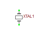
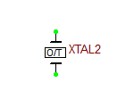
Crystal
This is a 2-pin parameterized crystal device.
Parameters:
| NAME | PARAMETER | UNITS | DEFAULT | NOTES |
|---|---|---|---|---|
| CM | motional capacitance | F | 10f | |
| C0 | shunt capacitance | F | 1p | |
| RM | motional resistance | Ohms | 100 | |
| LM | motional inductance | H | 100m |
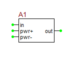
Current Limiter Block
The Current Limiter Block models the behavior of an operational amplifier or comparator device at a high level of abstraction. All of its pins act as inputs; three of the four also act as outputs. The model takes as input a voltage value from the âinâ connector. It then applies an offset and a gain, and derives from it an equivalent internal voltage (veq), which it limits to fall between pos pwr and neg pwr. If veq is greater than the output voltage seen on the âoutâ connector, a sourcing current will flow from the output pin. Conversely, if the voltage is less than vout, a sinking current will flow into the output pin. Depending on the polarity of the current flow, either a sourcing or a sinking resistance value (r_out_source, r_out_sink) is applied to govern the vout/i_out relationship. The chosen resistance will continue to control the output current until it reaches a maximum value specified by either i_limit_source or i_limit_sink. The latter mimics the current limiting behavior of many operational amplifier output stages. During all operation, the output current is reflected either in the pos_pwr connector current or the neg_pwr current, depending on the polarity of i_out. Thus, realistic power consumption as seen in the supply rails is included in the model. The user-specified smoothing parameters relate to model operation as follows: v_pwr_range controls the voltage below vpos_pwr and above vneg_pwr inputs beyond which veq [= gain * (vin + voffset)] is smoothed; i_source_range specifies the current below i_limit_source at which smoothing begins, as well as specifying the current increment above i_out=0.0 at which i_pos_pwr begins to transition to zero; i_sink_range serves the same purpose with respect to i_limit_sink and i_neg_pwr that i_source_range serves for i_limit_source & i_pos_pwr; r_out_domain specifies the incremental value above and below (veq-vout)=0.0 at which r_out will be set to r_out_source and r_out_sink, respectively. For values of (veq-vout) less than r_out_domain and greater than -r_out_domain, r_out is interpolated smoothly between r_out_source & r_out_sink.
Model Identifier: ilimit
Netlist Format:
A<device_name> <in_pin> <pos_pwr_pin> <neg_pwr_pin> <out_pin> <model_name>
.model <model_name> ilimit {<param1 = value> < param2 = value> ...}
Example:
A1 1 2 3 4 amp
.model amp ilimit in_offset=0.0 gain=16.0 r_out_source=1.0 r_out_sink=1.0 i_limit_source=1e-3 i_limit_sink=10e-3 v_pwr_range=0.2 i_source_range=1e-6 i_sink_range=1e-6 r_out_domain=1e-6
Parameters:
| NAME | PARAMETER | UNITS | DEFAULT | NOTES |
|---|---|---|---|---|
| in_offset | input offset | V | 0.0 | |
| gain | gain | - | 1.0 | |
| r_out_source | sourcing resistance | Ω | 1.0 | |
| r_out_sink | sinking resistance | Ω | 1.0 | |
| i_limit_source | current sourcing limit | A | 10m | |
| i_limit_sink | current sinking limit | A | 10m | |
| v_pwr_range | power smoothing range | V | 1u | |
| i_source_range | current sourcing smoothing range | A | 1n | |
| i_sink_range | current sinking smoothing range | A | 1n | |
| r_out_domain | output resistance smoothing domain | Ω | 1n |
Current Noise Source
This is a current noise generator characterized by a spectral density and corner frequency. You have to click the Edit Model... button to access the parameters of this device.
Parameters:
| NAME | PARAMETER | UNIT | DEFAULT | NOTES |
|---|---|---|---|---|
| En | noise current | A/âHz | 1p | required |
| freq | noise corner frequency | Hz | 100 | required |
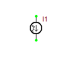
Current Source
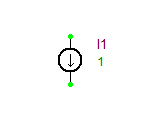
Current source has a DC value, a transient behavior, an AC behavior, and distortion parameters. The transient type, AC parameters, and distortion parameters are defined on the first tab of the source's property dialog. The transient expression can be a pulse, sinusoid, exponential, or piecewise linear. The DC value of a current source is its initial transient value. For a source with a sinusoidal transient behavior, for example, the DC value will be equal to its transient offset current. The AC parameters are magnitude and phase. These are used during the AC Frequency Sweep analysis. The distortion parameters, two sets of magnitude and phase, are used during the distortion analysis. The AC and distortion parameters are defined on the second tab of the source's property dialog.
Current-Controlled Switch
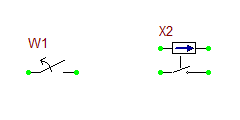
Switches are devices that exhibit high resistance when open (OFF state) and low resistance when closed (ON state). The switch model allows an almost ideal switch to be specified. With careful selection of the on and off resistances, they can effectively represent zero and infinite resistances in comparison to other circuit elements, while sustaining the model condition of a positive, finite value.
There are two versions of Current-Controlled Switch: two-terminal and four-terminal. For the two-terminal device, you must specify the name of the controlling Ammeter or voltage source, as well as the turn-on and turn-off currents in Amperes and on and off resistance values in Ohms. The four-terminal device already provides nodes for a controlling ammeter, and you just specify the rest of parameters. When the current through the switch or controlling device is greater or equal to the turn-on current, the switch closes. When the current through the switch or controlling device is less than or equal to the turn off current, the switch opens.
| NAME | PARAMETER | UNITS | DEFAULT | NOTES |
|---|---|---|---|---|
| I_ON | turn-on current | A | 0.0 | |
| I_OFF | turn-off current | A | 0.0 | |
| RON | closed resistance | Ohms | 1.0 | |
| ROFF | open resistance | Ohms | 1/GMIN |
D Flip-Flop
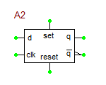
The digital D-type flip-flop is a one-bit, edge-triggered storage element which stores data whenever the clock (CLK) input line transitions from 0 (low) to 1 (high). In addition, there are asynchronous set and reset signals, which are independent of the clock. When SET = RESET = 0, the data on the D line is transferred to the output Q on the rising edge of the clock. The combination SET = 1 and RESET = 0, causes Q = 1. The combination SET = 0 and RESET = 1 causes Q = 0. The combination SET = RESET = 1 is illegal and is resolved by setting both outputs Q and Q_bar to 1.
Truth Table:
|
D Latch
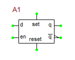
The digital D-type latch is a one-bit, level-sensitive storage element which outputs the value on the data (D) line whenever the enable (EN) input line is 1 (high). The value on the data line is stored, i.e., held on the output (Q) line whenever the enable (EN) line is 0 (low). In addition, there are set and reset signals, which are independent of the enable line. When SET = RESET = 0, the data on the D line is transferred to the output Q whenever EN = 1. The combination SET = 1 and RESET = 0, causes Q = 1. The combination SET = 0 and RESET = 1 causes Q = 0. The combination SET = RESET = 1 is illegal and is resolved by setting both outputs Q and Q_bar to 1.
Truth Table:
|
Darlington Pair
A Darlington pair is a three-pin device that consists of two interconnected BJT transistors of the same type. The collectors of two transistors are connected together to provide the "Collector" pin of the pair. The base of the first BJT acts the "Base" pin of the pair. The emitter of the first BJT is internally connected to the base of the second BJT. The emitter of the second BJT acts as the "Emitter" pin of the pair. There are two types of Darlington pair: NPN and PNP. The parameterized generic Darlington pair also contains a diode connected between the collector and emitter pin as well as two base-emitter resistors, one across each BJT.
Parameters:
| NAME | PARAMETER | UNITS | DEFAULT | NOTES |
|---|---|---|---|---|
| is_bjt | bjt saturation current | A | 1.0e-12 | |
| bf_bjt | bjt forward beta | - | 150 | |
| nf_bjt | bjt forward emission coefficient | - | 1 | |
| ise_bjt | B-E leakage saturation current | A | 0 | |
| ne_bjt | B-E leakage emission coefficient | - | 1 | |
| br_bjt | ideal maximum reverse beta | - | 1 | |
| nr_bjt | reverse current emission coefficient | - | 1 | |
| isc_bjt | B-C leakage saturation current | A | 0 | |
| nc_bjt | B-C leakage emission coefficient | - | 1 | |
| rb_bjt | zero bias base resistance | Ohms | 0 | |
| irb_bjt | current where base resistance falls halfway to minimum value | A | inf | |
| rbm_bjt | minimum base resistance at high currents | ohms | 0 | |
| re_bjt | emitter resistance | Ohms | 0 | |
| rc_bjt | collector resistance | Ohms | 0 | |
| cje_bjt | B-E zero bias depletion capacitance | F | 0 | |
| vje_bjt | B-E built-in potential | V | 0.75 | |
| mje_bjt | B-E junction grading coefficient | - | 0.33 | |
| cjc_bjt | B-C zero bias depletion capacitance | F | 0 | |
| vjc_bjt | B-C built-in potential | V | 0.75 | |
| mjc_bjt | B-C junction exponential factor | - | 0.33 | |
| tf_bjt | ideal forward transit time | sec | 0 | |
| tr_bjt | ideal reverse transit time | sec | 0 | |
| is_d | diode saturation current | A | 1.0e-12 | |
| rs_d | diode resistance | Ohms | 0 | |
| n_d | diode emission coefficient | - | 1 | |
| cjo_d | diode junction capacitance | F | 0 | |
| vj_d | diode junction potential | V | 1 | |
| m_d | diode grading coefficient | 0.5 | ||
| tnom | parameter measurement temperature | deg C | 27 | |
| r1 | first base-emitter resistance | Ohms | 1k | |
| r2 | second base-emitter resistance | Ohms | 1k |
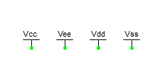
DC Bias Sources Vcc, Vee, Vdd, Vss
These are simple 1-pin DC voltage sources. Vcc and Vdd provide a positive voltage, while Vee and Vss provide a negative voltage
Parameters:
| NAME | PARAMETER | UNIT | DEFAULT | NOTES |
|---|---|---|---|---|
| vcc | bias voltage | V | +15 | required |
| vee | bias voltage | V | -15 | required |
| vdd | bias voltage | V | +15 | required |
| vss | bias voltage | V | -15 | required |
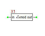
Delta Modulator Block
This device samples an input signal at the specified sampling period and generates a Delta modulated output signal from it.
Parameters:
| NAME | PARAMETER | UNITS | DEFAULT | NOTES |
|---|---|---|---|---|
| r_in | input resistance | Ω | 1G | |
| r_out | output resistance | Ω | 1u | |
| T | sampling period | sec | 1 | |
| duty_cycle | sampling pulse duty cycle | - | 0.01 |
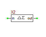
Delta-Sigma Modulator Block
This device samples an input signal at the specified sampling period and generates a Delta-Sigma modulated output signal from it.
Parameters:
| NAME | PARAMETER | UNITS | DEFAULT | NOTES |
|---|---|---|---|---|
| r_in | input resistance | Ω | 1G | |
| r_out | output resistance | Ω | 1u | |
| T | sampling period | sec | 1 | |
| duty_cycle | sampling pulse duty cycle | - | 0.01 |
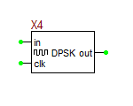
Differential Phase Shift-Keying Modulator Block
This device takes a digital input like a binary sequence and generates a DPSK modulated output signal with two specified carrier phase values. It also requires a digital clock input for synchronization.
Parameters:
| NAME | PARAMETER | UNITS | DEFAULT | NOTES |
|---|---|---|---|---|
| r_out | output resistance | Ω | 1u | |
| phi_lo | low carrier phase value | rad | 0 | |
| phi_hi | high carrier phase value | rad | Ï | |
| fc | carrier frequency | Hz | 1Meg | |
| ac | carrier peak amplitude | V | 1.0 |
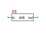
Differentiator Block
The Differentiator Block approximates the time derivative of an input signal by calculating the incremental slope of that signal since the previous time point. Gain and output offset parameters are also included to allow for tailoring of the required signal. Output upper and lower limits are also included to prevent convergence erros resulting from excessively large output values. The incremental value of output below the output_upper_limit and above the output_lower_limit at which smoothing begins is specified via the limit_range parameter. In AC analysis, the value returned is equal to the radian frequency of analysis multiplied by the gain.
Model Identifier: d_dt
Netlist Format:
A<device_name> <in_pin> <out_pin> <model_name>
.model <model_name> d_dt out_lower_limit = <value> out_upper_limit = <value> {<param1 = value> < param2 = value> ...}
Example:
A1 1 2 differentiator
.model differentiator d_dt out_lower_limit = -1t out_upper_limit = 1t
Parameters:
| NAME | PARAMETER | UNITS | DEFAULT | NOTES |
|---|---|---|---|---|
| gain | gain | - | 1.0 | |
| out_offset | output offset | V | 0.0 | |
| out_lower_limit | output lower limit | V | -1t | required |
| out_upper_limit | output upper limit | V | 1t | required |
| limit_range | upper and lower limit smoothing range | - | 1.0e-6 |
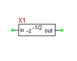
Digital Integrator Block
This device models a digital integrator with a Z-transform of -z-1/2, which is equivalent to a delay line with a delay of half the sampling period
Parameters:
| NAME | PARAMETER | UNITS | DEFAULT | NOTES |
|---|---|---|---|---|
| T | sampling period | sec | 1 | required |
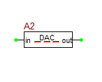
Digital-to-Analog Converter (DAC) Bridge
The DAC Bridge takes a digital value from a digital node and can only be eiter "0", "1", or "U". It then outputs the value "out_low", "out_high" or "out_udndef", or ramps linearly toward one of these "final" values from its curent analog output level. This ramping speed depends on the values of "t_rise" and "t_fall".
Model Identifier: dac_bridge
Netlist Format:
A<device_name> [<in_pin> {<in2_pin>> ...}] [<out_pin> {<out2_pin> ...}] <model_name>
.model <model_name> dac_bridge {<param1 = value> < param2 = value> ...}
Example:
A [1] [2] dac_bridge
.model dac_bridge dac_bridge out_low = 0 fall_delay = 1n
Parameters:
| NAME | PARAMETER | UNIT | DEFAULT | NOTES |
|---|---|---|---|---|
| out_low | analog output for 0 digital input | V | 0 | required |
| out_high | analog output for 1 digital input | V | 1 | required |
| out_undef | analog output for undefined digital input | V | 0.5 | required |
| input_load | capacitive input load | F | 1p | |
| t_rise | L-to-H delay time | sec | 1n | |
| t_fall | H-to-L delay time | sec | 1n |
Diode
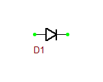
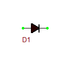
Diodes allow current flow only in one direction, following their symbol's arrow, and thus can be used as simple solid state switches in AC circuits.
The standard device parameters are AREA, OFF, IC, and T. They are described below:
| AREA | area factor (optional) (If not specified, the default value is 1.0.) |
| OFF | initial condition for the DC analysis (optional) |
| IC | initial condition (optional) (Used when a transient analysis is desired, which starts from other than the quiescent operating point.) |
| T | operating temperature of the device (optional) |
The process models can be either junction diodes or Schottky barrier diodes. Area factor scales the model parameters IS, RS, CJO, and IBV. VD is the initial voltage, and TEMP is the overriding temperature. Descriptions of the process model parameters are given in the following table:
| NAME | PARAMETER | UNITS | DEFAULT | NOTES |
|---|---|---|---|---|
| IS | saturation current | A | 1e-14 | |
| TNOM | parameter measurement temperature | deg C | 27 | |
| RS | ohmic resistance | Ohms | 0 | |
| N | emission coefficient | - | 1 | |
| TT | transit-time | sec | 0 | |
| CJO | zero-bias junction capacitance | F | 0 | |
| VJ | junction potential | V | 1 | |
| M | grading coefficient | - | 0.5 | |
| EG | activation energy | eV | 1.11 | |
| XTI | saturation current temp. exp. | - | 3.0 | |
| KF | flicker noise coefficient | - | 0 | |
| AF | flicker noise exponent | - | 1 | |
| FC | forward bias junction fit parameter | - | 0.5 | |
| BV | reverse breakdown voltage | V | inf | |
| IBV | current at breakdown voltage | A | 1e-3 |
Diode Bridge
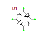
This four-pin device is a bridge configuration of four generic diodes.
Parameters:
| NAME | PARAMETER | UNITS | DEFAULT | NOTES |
|---|---|---|---|---|
| IS | saturation current | A | 1e-14 | |
| RS | ohmic resistance | Ohms | 0 | |
| N | emission coefficient | - | 1 | |
| TT | transit-time | sec | 0 | |
| CJO | zero-bias junction capacitance | F | 10p | |
| VJ | junction potential | V | 1 | |
| M | grading coefficient | - | 0.5 | |
| BV | reverse breakdown voltage | V | 1000 | |
| IBV | current at breakdown voltage | A | 1e-3 | |
| TNOM | parameter measurement temperature | deg C | 27 |
Discrete Convolution Block
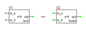
These blocks perform an N-point discrete convolution of their input signals. Both of the input signals x(t) and h(t) are sampled at the specified sampling period. The samples of x(t) are then shifted in time for the convolution. The output signal is a pulse train of the same period with the specified duty cycle. The input signal of these block can be either continuous-time signals or pulse trains of the specified period.
Parameters:
| NAME | PARAMETER | UNITS | DEFAULT | NOTES |
|---|---|---|---|---|
| T | sampling period | sec | 1 | required |
| rise_time | window rise time | sec | 0 | |
| fall_time | window fall time | sec | 0 | |
| duty_cycle | output pulse duty cycle | - | 0.1 | |
| gain | output gain | - | 1 |
Discrete Fourier Transform (DFT) Block
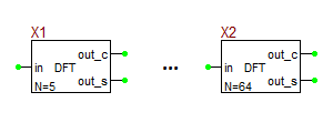
These blocks perform an M-point discrete Fourier transform (DFT) of their input signal and then sample each period of the Fourier transform N times in the frequency domain. The output signals are two finite sequence pulse trains representing the cosine and sine DFT transforms. The input signal of these block can be either a continuous-time signal or a pulse train of the specified period.
There are ten DFT blocks for M = 5, 6, 7, 8, 9, 10, 12, 16, 32, 64. In each case, the total duration of the transform window is MT, where T is the sampling period. By default, the frequency domain sampling starts at t = MT and takes place over one spectral period equal to fs = 1/T. You can change the sampling start time by "n_delay" temporal periods. n_delay = 0 by default, but it can be either positive or negative. You can also extend spectral sampling to more than one spectral period by increasing the value of the parameter "n_dur", which has a default value of 1.
Parameters:
| NAME | PARAMETER | UNITS | DEFAULT | NOTES |
|---|---|---|---|---|
| T | sampling period | sec | 1 | required |
| N | sequence length | - | 5 | required |
| rise_time | window rise time | sec | 0 | |
| fall_time | window fall time | sec | 0 | |
| duty_cycle | output pulse duty cycle | - | 0.1 | |
| n_delay | number of delayed period before sampling | - | 0 | |
| n_dur | number of frequency-sampled periods | - | 1 |
Discrete-Time Fourier Transform (DTFT) Block
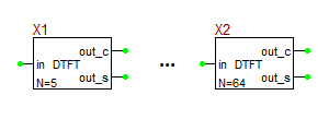
These blocks perform an N-point discrete-time Fourier transform (DTFT) of their input signal and output the transform as two temporal voltage signals representing the cosine and sine DTFT transforms. The The input signal of these block can be either a continuous-time signal or a pulse train of the specified period.
There are ten DTFT blocks for N = 5, 6, 7, 8, 9, 10, 12, 16, 32, 64. In each case, the total duration of the transform window is NT, where T is the sampling period.
Parameters:
| NAME | PARAMETER | UNITS | DEFAULT | NOTES |
|---|---|---|---|---|
| T | sampling period | sec | 1 | required |
| rise_time | window rise time | sec | 0 | |
| fall_time | window fall time | sec | 0 |
Discrete-Time Signal Hold Block
This device takes a pulse train of a specified period as its input and holds the value of each pulse's amplitude during each clock cycle at the output.
Parameters:
| NAME | PARAMETER | UNITS | DEFAULT | NOTES |
|---|---|---|---|---|
| T | sampling period | sec | 1 | required |
| duty_cycle | sampling pulse duty cycle | - | 0.1 | |
| rise_time | window rise time | sec | 0 | |
| fall_time | window fall time | sec | 0 | |
| Tmax | signal period or maximum duration | sec | 10 |
Divider Block
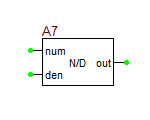
The Divider Block has two inputs. Each of the numerator and denominator inputs is added to its respective offset and then multiplied by its respective input gain (with default values of 1). Next, the loaded numerator signal is divided by the loaded denominator signal. The result is multiplied by the output gain and then added to the output offset. To avoid division by zero, the divider function sets the denominator signal greater than zero through the lower limit parameter. This limit is approached through a quadratic smoothing function, the domain of which may be specified as a fraction of the lower limit value or as an absolute value. The divider function operates in DC, AC, and Transient analysis modes. In AC analysis, however, it is important to remember that results are invalid unless the denominator input is a DC voltage.
Model Identifier: divide
Netlist Format:
A<device_name> <num_pin> <den_pin> <out_pin> <model_name>
.model <model_name> divide {<param1 = value> < param2 = value> ...}
Example:
A1 1 2 3 divider_block
.model divider_block divide den_offset = 0.0 den_gain = 1.0
Parameters:
| NAME | PARAMETER | UNITS | DEFAULT | NOTES |
|---|---|---|---|---|
| num_offset | numerator offset | V | 0.0 | |
| num_gain | numerator gain | - | 1.0 | |
| den_offset | denominator offset | V | 0.0 | |
| den_gain | denominator gain | - | 1.0 | |
| den_lower_limit | denominator lower limit | V | 1.0e-10 | |
| den_domain | denominator smoothing domain | - | 1.0e-10 | |
| fraction | smoothing fraction/absolute value switch | - | False | |
| out_gain | output gain | - | 1.0 | |
| out_offset | output offset | V | 0.0 |
Double-Layer CPW Line
This is a four-pin, two-port device that models a coplanar waveguide (CPW) line segment on a double-layer dielectric substrate without a ground backing.
Model Identifier: cpw-doublelayer
Parameters:
| NAME | PARAMETER | UNITS | DEFAULT | NOTES |
|---|---|---|---|---|
| w | slot width | mm | 2.0 | |
| s | center strip width | mm | 2.0 | |
| h1 | lower layer substrate thickness | mm | 1.6 | |
| er1 | lower layer substrate relative permittivity | - | 2.2 | |
| h2 | upper layer substrate thickness | mm | 1 | |
| er2 | upper layer substrate relative permittivity | - | 3.0 | |
| len | cpw line length | mm | 10 |
Doubly Center-Tapped Ferrite Core Transformer
This six-pin four-port device models a doubly center-tapped physical transformer with a magnetic ferrite core. Its model is based on XSPICE's magnetic core and inductive coupling models. For this device you need to specify physical parameters like cross sectional area, core length and number of primary and secondary turns. The physical model of the magnetic device is defined by two vectors: magnetic field intensity H in A/m and magnetic flux density B (also known as magnetic induction) in Tesla. The default array values are:
H_array = [-250 -100 -50 -37.5 -25 -12.5 0 12.5 25 37.5 50 100 250]
B_array = [-0.375 -0.36 -0.32 -0.29 -0.24 -0.15 0 0.15 0.24 0.29 0.32 0.36 0.375]
To change the value of H/B arrays, open the subcircuit model dialog by clicking the View Subcircuit button and edit its text.
Parameters:
| NAME | PARAMETER | UNITS | DEFAULT | NOTES |
|---|---|---|---|---|
| n_prim | number of full-winding primary inductor coupling turns | - | 100 | required |
| n_sec | number of full-winding secondary inductor coupling turns | - | 100 | required |
| area | cross-sectional area | m2 | 1e-5 | |
| length | core length | m | 0.01 |
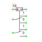
DPDT Switch
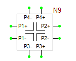
This is an 8-pin device that models a double-pole double-throw switch. It has two input signals and four output pins. When the control voltage is at the high state, the first and second input voltages are transferred to the first and third output pins, respectively. When the control voltage is at the low state, the first and second input voltages are transferred to the second and fourth output pins, respectively.
Parameters:
| NAME | PARAMETER | UNITS | DEFAULT | NOTES |
|---|---|---|---|---|
| von | turn-on voltage | V | 3.3 | |
| voff | turn-off voltage | V | 0.3 | |
| vt | threshold voltage | V | 1.0 | |
| ron | on resistance | Ohms | 1.0 | |
| roff | off resistance | Ohms | 1Gig |
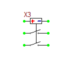
DPST Switch
This is a 6-pin device that models a double-pole single-throw switch. It has two input signals and two output signals. When the switch on, the first and second input voltages are transferred to the first and second output pins, respectively. When the switch is off, the output pin do not receive any input signals.
Parameters:
| NAME | PARAMETER | UNITS | DEFAULT | NOTES |
|---|---|---|---|---|
| von | turn-on voltage | V | 3.3 | |
| voff | turn-off voltage | V | 0.3 | |
| vt | threshold voltage | V | 1.0 | |
| ron | on resistance | Ohms | 1.0 | |
| roff | off resistance | Ohms | 1Gig |
Ferrite Core Transformer
This four-pin two-port device models a physical transformer with a magnetic ferrite core. Its model is based on XSPICE's magnetic core and inductive coupling models. For this device you need to specify physical parameters like cross sectional area, core length and number of primary and secondary turns. The physical model of the magnetic device is defined by two vectors: magnetic field intensity H in A/m and magnetic flux density B (also known as magnetic induction) in Tesla. The default array values are:
H_array = [-250 -100 -50 -37.5 -25 -12.5 0 12.5 25 37.5 50 100 250]
B_array = [-0.375 -0.36 -0.32 -0.29 -0.24 -0.15 0 0.15 0.24 0.29 0.32 0.36 0.375]
To change the value of H/B arrays, open the subcircuit model dialog by clicking the View Subcircuit button and edit its text.
Parameters:
| NAME | PARAMETER | UNITS | DEFAULT | NOTES |
|---|---|---|---|---|
| n_prim | number of primary turns | - | 100 | required |
| n_sec | number of secondary turns | - | 100 | required |
| area | cross-sectional area | m2 | 1e-5 | |
| length | core length | m | 0.01 |
Finite Sequence Pulse Generator
This is a voltage source that generates a pulse train of finite duration oscillating between zero and a user defined maximum voltage level.
Parameters:
| NAME | PARAMETER | UNIT | DEFAULT | NOTES |
|---|---|---|---|---|
| T | pulse period | sec | 1m | required |
| w | pulse width | sec | 0.5m | required |
| n | number of pulses | - | 5 | |
| rise_time | pulse rise time | sec | 0 | |
| fall_time | pulse fall time | sec | 0 | |
| max_val | maximum output voltage level | V | 1 | |
| start | start time | sec | 0 |
Finite Sequence Random Pulse Generator
This is a voltage source that generates a finite sequence of random pulses with a user defined number of random levels. By default, both the pulse amplitude and pulse width are randomized. You have the option to fix either of these parameters.
Parameters:
| NAME | PARAMETER | UNIT | DEFAULT | NOTES |
|---|---|---|---|---|
| period | period | sec | 1 | required |
| duty_cycle | pulse duty cycle | - | 0.5 | required |
| random_amp | 1 for random amplitude, 0 otherwise | - | 1 | |
| random_wid | 1 for random pulse width, 0 otherwise | - | 1 | |
| n_rand | number of random levels | - | 10 | |
| rise_time | pulse rise time | sec | 0 | |
| fall_time | pulse fall time | sec | 0 | |
| max_val | maximum output voltage level | V | 1 | |
| n_val | number of random pulses | - | 5 | |
| start | start time | sec | 0 |
Finite Sequence Signal Sampler Block
This device samples its input signal during a finite time window at a specified sampling period and outputs a pulse train of finite duration with a specified duty cycle.
Parameters:
| NAME | PARAMETER | UNITS | DEFAULT | NOTES |
|---|---|---|---|---|
| T | sampling period | sec | 1 | required |
| duty_cycle | sampling pulse duty cycle | - | 0.01 | |
| rise_time | window rise time | sec | 0 | |
| fall_time | window fall time | sec | 0 | |
| n | number of samples | - | 5 | |
| start | start time | sec | 0 |
Finite-Ground Coplanar Waveguide (FGCPW) Line
This is a four-pin, two-port device that models a coplanar waveguide (CPW) line segment with top ground strips of finite width on a single-layer dielectric substrate without a ground backing.
Model Identifier: fgcpw-line
Parameters:
| NAME | PARAMETER | UNITS | DEFAULT | NOTES |
|---|---|---|---|---|
| w | slot width | mm | 2.0 | |
| s | center strip width | mm | 2.0 | |
| g | ground strip width | mm | 5.0 | |
| h | substrate thickness | mm | 1.6 | |
| er | substrate relative permittivity | - | 2.2 | |
| len | cpw line length | mm | 10.0 |
FM Modulated Source
This is a voltage source with a single-tone frequency modulated waveform. The FM modulation index MDI is defined as the ratio of maximum frequency deviation to maximum signal amplitude.
Parameters:
| NAME | PARAMETER | UNIT | DEFAULT | NOTES |
|---|---|---|---|---|
| V0 | offset | V | 0 | |
| VA | amplitude | V | 1 | |
| FC | carrier frequency | Hz | 1 | required |
| MDI | modulation index | - | 0 | required |
| FS | signal frequency | Hz | 1 | required |
Frequency Detector Block
This device measures the frequency of a harmonic input signal and produces a voltage proportional to the frequency in Hz at the output. It can also be used as a frequency converter.
Parameters:
| NAME | PARAMETER | UNITS | DEFAULT | NOTES |
|---|---|---|---|---|
| r_in | input resistance | Ω | 1G | |
| r_out | output resistance | Ω | 1u | |
| K_v | voltage conversion factor | V/Hz | 1e-6 | |
| max_in | input amplitude | V | 1 |
Frequency Doubler Block
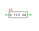
This device takes a harmonic input signal and generates a harmonic output signal with twice the frequency and a user specified amplitude.
Parameters:
| NAME | PARAMETER | UNITS | DEFAULT | NOTES |
|---|---|---|---|---|
| r_in | input resistance | Ω | 1G | |
| r_out | output resistance | Ω | 1u | |
| max_val | output amplitude | V | 1.0 |
Frequency Down-Converter Block
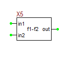
This 3-pin device takes two harmonic input signals with different frequencies fLO and fIF and generates a harmonic output signal with a frequency equal to fRF = fLO - fIF and a user specified amplitude.
Parameters:
| NAME | PARAMETER | UNITS | DEFAULT | NOTES |
|---|---|---|---|---|
| r_in | input resistance | Ω | 1G | |
| r_out | output resistance | Ω | 1u | |
| max_in | peak amplitude of both inputs | V | 1.0 | Both inputs must have equal amplitudes. |
| max_out | output amplitude | V | 1.0 |
Frequency Meter
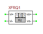
The Frequency Meter is a four-pin shunt device that is connected in parallel with an AC source just like a voltmeter and measures the operating frequency of the AC circuit. The input pins are connected across the AC source. The voltage across the output pins is equal to the frequency of the source in Hertz within a scale factor SF. Note that the Frequency Meter is designed to work with a single-tone AC source of unit amplitude. If the amplitude of the source is not one, multiply the SF parameter by the non-unit source amplitude value. The output voltage of the Frequency Meter can be used in conjunction with linear or nonlinear dependent sources to model frequency-dependent quantities.
Model Identifier: fmeter
Parameters:
The only parameter is the scale factor SF with a default value of 1.0. Set SF = 1e-6 to read out the frequency in MHz. Set SF = 1e-9 to read out the frequency in GHz. Set SF = 6.283185 (2*pi) to read out the angular frequency Ï in radian/s.
Frequency Modulator Block
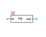
This device takes an input signal and generates an FM modulated output signal of a specified carrier frequency with a specified maximum frequency deviation.
Parameters:
| NAME | PARAMETER | UNITS | DEFAULT | NOTES |
|---|---|---|---|---|
| r_in | input resistance | Ω | 1G | |
| r_out | output resistance | Ω | 1u | |
| f_del | maximum frequency deviation | Hz | 500k | |
| fc | carrier frequency | Hz | 1Meg | |
| ac | carrier peak amplitude | V | 1 |
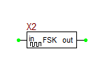
Frequency Shift-Keying Modulator Block
This device takes a digital input like a binary sequence and generates an FSK modulated output signal with two specified carrier frequencies.
Parameters:
| NAME | PARAMETER | UNITS | DEFAULT | NOTES |
|---|---|---|---|---|
| r_out | output resistance | Ω | 1u | |
| fc_lo | low carrier frequency | Hz | 1Meg | |
| fc_hi | high carrier frequency | Hz | 2Meg | |
| ac | carrier peak amplitude | V | 1.0 |
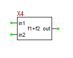
Frequency Up-Converter Block
This 3-pin device takes two harmonic input signals with different frequencies fLO and fIF and generates a harmonic output signal with a frequency equal to fRF = fLO + fIF and a user specified amplitude.
Parameters:
| NAME | PARAMETER | UNITS | DEFAULT | NOTES |
|---|---|---|---|---|
| r_in | input resistance | Ω | 1G | |
| r_out | output resistance | Ω | 1u | |
| max_in | peak amplitude of both inputs | V | 1.0 | both inputs must have equal amplitudes. |
| max_out | output amplitude | V | 1.0 |
Fuse
This is a 2-pin interactive current-controlled switch. If the current passing through the fuse is less than a specified threshold current, the switch is closed. If the current exceeds the threshold level, the fuse breaks and remains open thereafter. The device's symbol changes to display its state.
Parameters:
| NAME | PARAMETER | UNITS | DEFAULT | NOTES |
|---|---|---|---|---|
| r | resistance when intact | Ohms | 1.0 | |
| i_thresh | threshold current | A | 1.0 |
Gain Block
This model is a simple gain block with optional offsets on the input and the output. In_offset is added to the input, the sum of which is then multiplied by the gain, and the output offset is added to produce the final output. The gain block model will operate in DC, AC, and Transient analysis modes.
Model Identifier: gain
Netlist Format:
A<device_name> <in_pin> <out_pin> <model_name>
.model <model_name> gain {<param1 = value> < param2 = value> ...}
Example:
A1 1 2 gain_block
.model gain_block gain in_offset = 0.0 out_offset = 0.0
Parameters:
| NAME | PARAMETER | UNITS | DEFAULT | NOTES |
|---|---|---|---|---|
| in_offset | input offset | V | 0.0 | |
| gain | gain | - | 1.0 | |
| out_offset | out_offset | V | 0.0 |
Generalized Analog Filter Block
This block models a generalize analog filter characterized by a rational transfer functions in the spectral domain Laplace variable s:
[math] H(s) = \frac{N(s)}{D(s)} = \frac{ \sum_{m=0}^{M} b_m s^m }{ \sum_{n=0}^{N} a_n s^n } [/math]
subject to the requirement N ⥠M and aN = 1. To access the parameters of this block, you have to click the Edit Model... button of its property dialog.
The functionality of this block, which is native to RF.Spice A/D, is very similar to the s-domain transfer function block, which is an XPSICE process model. This block does not have a denormalization frequency parameter. Therefore, at frequencies other than the unit frequency, the transfer function must be explicitly scaled. This block can be used in conjunction with both transient and AC frequency sweep tests.
Parameters:
| NAME | PARAMETER | UNITS | DEFAULT | NOTES |
|---|---|---|---|---|
| deg | highest degree of s in transfer function | - | 2 | required |
| coeff_den | denominator coefficients array: coefficients of powers of s, highest power first | - | 1 0 1 | required |
| coeff_num | numerator coefficients array: coefficients of powers of s, highest power first | - | 0 0 1 | required |
| r_in | input resistance | Ω | 10G | |
| r_out | output resistance | Ω | 1u |
Generalized Digital Filter Block
This block models a generalized digital filter characterized by a rational transfer functions in the Z-transform domain variable z:
[math] H(z) = \frac{N(z)}{D(z)} = \frac{ \sum_{m=0}^{M} b_m z^m }{ \sum_{n=0}^{N} a_n z^n } [/math]
subject to the requirement N ⥠M. To access the parameters of this block, you have to click the Edit Model... button of its property dialog.
Parameters:
| NAME | PARAMETER | UNITS | DEFAULT | NOTES |
|---|---|---|---|---|
| deg | highest degree of z in transfer function | - | 2 | required |
| coeff_den | denominator coefficients array: coefficients of powers of (-z1/2), highest power first | - | 1 0 1 0 1 | required |
| coeff_num | numerator coefficients array: coefficients of powers of (-z1/2), highest power first | - | 1 0 0 0 0 | required |
| freq | sampling frequency | Hz | 1 | required |
Generic Bandpass Filter Block
This device is a generic bandpass filter with user specified center frequency and bandwidth. It is based on a fifth-order Butterworth LC ladder topology.
Parameters:
| NAME | PARAMETER | UNITS | DEFAULT | NOTES |
|---|---|---|---|---|
| f0 | center frequency | Hz | 1Meg | |
| bw | bandwidth | Hz | 200k | |
| r0 | source/load resistance | Ω | 50 |
Generic Bandstop Filter Block
This device is a generic bandstop filter with user specified center frequency and bandwidth. It is based on a fifth-order Butterworth LC ladder topology.
Parameters:
| NAME | PARAMETER | UNITS | DEFAULT | NOTES |
|---|---|---|---|---|
| f0 | center frequency | Hz | 1Meg | |
| bw | bandwidth | Hz | 200k | |
| r0 | source/load resistance | Ω | 50 |
Generic Bend Junction
This is a four-pin, two-port device that models a bend in a general purpose transmission line. The bend geometry and the line structure can be very complicated, and their full-wave effects can be captured by the measured or simulated S-parameter data of this device. The model may also include a certain length of the transmission line at the input and output ports.
Model Identifier: bend-junction
Parameters:
A table of s11, s21, s12 and s22-parameter values as a function of frequency
Generic Coupled T-Lines
This is an eight-pin, four-port device that models a two parallel general purpose coupled transmission line segments. Ports 1 and 2 represent the input and output of the first T-Line. Ports 3 and 4 represent the input and output of the second coupled T-Line.
Model Identifier: coupled-lines
Parameters:
| NAME | PARAMETER | UNITS | DEFAULT | NOTES |
|---|---|---|---|---|
| Z0e | even mode characteristic impedance | Ohms | 50.0 | |
| Z0o | odd mode characteristic impedance | Ohms | 10.0 | |
| eeff | effective permittivity | - | 1.0 | |
| len | line segment length | mm | 10.0 |
Generic Cross Junction
This is an eight-pin, four-port device that models a cross junction among four general purpose transmission lines. The cross geometry and the line structures can be very complicated, and their full-wave effects can be captured by the measured or simulated S-parameter data of this device. The model may also include a certain length of the four transmission lines at the four ports.
Model Identifier: tee-junction
Parameters:
A table of s11, s21, s31, s41, s12, s22, s32, s42, s13, s23, s33, s43, s14, s24, s34 and s44-parameter values as a function of frequency
Generic Highpass Filter Block
This device is a generic highpass filter with a user specified cutoff frequency. It is based on a fifth-order Butterworth LC ladder topology.
Parameters:
| NAME | PARAMETER | UNITS | DEFAULT | NOTES |
|---|---|---|---|---|
| cutoff | cutoff frequency | Hz | 1Meg | |
| r0 | source/load resistance | Ω | 50 |
Generic Lowpass Filter Block
This device is a generic lowpass filter with a user specified cutoff frequency. It is based on a fifth-order Butterworth LC ladder topology.
Parameters:
| NAME | PARAMETER | UNITS | DEFAULT | NOTES |
|---|---|---|---|---|
| cutoff | cutoff frequency | Hz | 1Meg | |
| r0 | source/load resistance | Ω | 50 |
Generic Multiport Networks
RF.Spice A/D currently offers four types of generic network devices: one-port, two-port, three-port and four-port. There are two-pin, four-pin, six-pin and eight-pin, respectively. Multiport networks can be used to model very complicated active or passive structures, which can be characterized by their measured or simulated S-parameter data.
Model Identifier: one-port, two-port, three-port, four-port
Parameters:
One-Port: A table of s11-parameter values as a function of frequency
Two-Port: A table of s11, s21, s12 and s22-parameter values as a function of frequency
Three-Port: A table of s11, s21, s31, s12, s22, s32, s13, s23 and s33-parameter values as a function of frequency
Four-Port: A table of s11, s21, s31, s41, s12, s22, s32, s42, s13, s23, s33, s43, s14, s24, s34 and s44-parameter values as a function of frequency
Generic Open End
This is a two-pin, one-port device that models the open end of a general purpose transmission line segment. Infringing capacitance effects can be captured by the measured or simulated S-parameter data of this device. The model may also include a certain length of the transmission line.
Model Identifier: open-end
Parameters:
A table of s11-parameter values as a function of frequency
Generic Open Stub
This is a two-pin, one-port device that models a general purpose transmission line segment terminated in an open end. An infinite impedance load is indeed connected to the end of the T-line segment. The fringing capacitance effects, however, are neglected by this model.
Model Identifier: stub-open
Parameters:
| NAME | PARAMETER | UNITS | DEFAULT | NOTES |
|---|---|---|---|---|
| Z0 | characteristic impedance | Ohms | 50.0 | |
| eeff | effective permittivity | - | 1.0 | |
| alpha | attenuation constant | dB/m | 0.0 | |
| len | line segment length | mm | 10.0 |
Generic Short Stub
This is a two-pin, one-port device that models a general purpose transmission line segment terminated in a shorted end. A zero impedance load is indeed connected to the end of the T-line segment. The inductive loading effects, however, are neglected by this model.
Model Identifier: stub-short
Parameters:
| NAME | PARAMETER | UNITS | DEFAULT | NOTES |
|---|---|---|---|---|
| Z0 | characteristic impedance | Ohms | 50.0 | |
| eeff | effective permittivity | - | 1.0 | |
| alpha | attenuation constant | dB/m | 0.0 | |
| len | line segment length | mm | 10.0 |
Generic Step Junction
This is a four-pin, two-port device that models a step-in-width junction between two general purpose transmission lines. The step geometry and the line structures can be very complicated, and their full-wave effects can be captured by the measured or simulated S-parameter data of this device. The model may also include a certain length of the two transmission lines at the input and output ports.
Model Identifier: step-junction
Parameters:
A table of s11, s21, s12 and s22-parameter values as a function of frequency
Generic T-Line
This is a four-pin, two-port device that models a general purpose transmission line segment.
Model Identifier: t-line
Parameters:
| NAME | PARAMETER | UNITS | DEFAULT | NOTES |
|---|---|---|---|---|
| Z0 | characteristic impedance | Ohms | 50.0 | |
| eeff | effective permittivity | - | 1.0 | |
| alpha | attenuation constant | dB/m | 0.0 | |
| len | line segment length | mm | 10.0 |
Generic Tee Junction
This is a six-pin, three-port device that models a tee junction among three general purpose transmission lines. The tee geometry and the line structures can be very complicated, and their full-wave effects can be captured by the measured or simulated S-parameter data of this device. The model may also include a certain length of the three transmission lines at the two through ports and the side arm.
Model Identifier: tee-junction
Parameters:
A table of s11, s21, s31, s12, s22, s32, s13, s23 and s33-parameter values as a function of frequency
Geometric Mean Block
This 3-pin device sends the geometric mean of its two inputs to the output with a default unity gain.
Parameters:
| NAME | PARAMETER | UNITS | DEFAULT | NOTES |
|---|---|---|---|---|
| gain | gain | - | 1.0 |
Ground
Ground has a voltage of zero (0) and is used as a reference to compute electrical values in the circuit. All circuits must be grounded to be properly simulated. There is no limit on the number of grounds you may use in a circuit. All components connected to ground are referenced to a common point and treated as linked through ground.
Gudermannian Polarity Detector Block
This 3-pin device measures the difference signal Îv = vpos - vneg and produces an output proportional to the Gudermannian function of Îv:
[math] v_{out} = A \cdot \frac{2}{\pi} \ gd(a\Delta v) = A \cdot \left( \frac{4}{\pi} \tan^{-1}(e^{a\Delta v}) - 1 \right) [/math]
Parameters:
| NAME | PARAMETER | UNITS | DEFAULT | NOTES |
|---|---|---|---|---|
| a | shaping Constant | - | 10 | |
| MaxVal | output amplitude | V | 1 |
Hysteresis Block (XSPICE)
The Hysteresis block is a simple buffer stage that provides hysteresis of the output with respect to the input. The in_low and in_high parameter values. The output values are limited to out_lower_limit and out_upper_limit. The value of \93hyst\94 is added to the in_low and in_high points in order to specify the points at which the slope of the hysteresis function would normally change abruptly as the input transitions from a low to a high value. Likewise, the value of \93hyst\94 is subtracted from the in_high and in_low values in order to specify the points at which the slope of the hysteresis function would normally change abruptly as the input transitions from a high to a low value. In fact, the slope of the hysteresis function is never allowed to change abruptly but is smoothly varied whenever the input_dowmain smoothing parameter is set greater than zero.
Model Identifier: hyst
Netlist Format:
A<device_name> <in_pin> <out_pin> <model_name>
.model <model_name> hyst {<param1 = value> < param2 = value> ...}
Example:
A1 1 2 hysteresis_block
.model hysteresis_block hyst in_low = 0.0 in_high = 1.0
Parameters:
| Name | Description | Default |
|---|---|---|
| In_low | input low value | 0.0 |
| in_high | input high value | 1.0 |
| hyst | hysteresis | 0.1 |
| out_lower_limit | output lower limit | 0.0 |
| out_upper_limit | output upper limit | 1.0 |
| input_domain | input smoothing domain | 0.01 |
| fraction | smoothing fraction/absolute value switch | true |
Ideal Buffer Block
This model is an ideal buffer block with a default unity gain.
Parameters:
| NAME | PARAMETER | UNITS | DEFAULT | NOTES |
|---|---|---|---|---|
| r_in | input resistance | Ω | 1G | |
| r_out | output resistance | Ω | 1u | |
| gain | gain | - | 1.0 |
Ideal Center-Tapped Transformer with Push-Pull Input
The ideal center-tapped transformer with push-pull input is a five-pin three-port device with two primary input ports and one secondary output port. Its model is based on the Ideal Transformer, and the relationship between its primary and secondary voltages is given by:
[math] \frac{v_P1}{v_S} = \frac{v_P2}{v_S} = n [/math]
where vS is the secondary voltage, vP1 is measured between the top primary pin P1 and the center tap pin, and vP2 is measured between the center tap pin and the bottom primary pin P2. The red dots show the polarity of the windings on each side. This model has one parameter: ratio = n = NP1/NS = NP2/NS, which represents the primary-to-secondary (half-winding) turns ratio.
Ideal Center-Tapped Transformer with Push-Pull Output
The ideal center-tapped transformer with push-pull output is a five-pin three-port device with one primary input port and two secondary output ports. Its model is based on the Ideal Transformer, and the relationship between its primary and secondary voltages is given by:
[math] \frac{v_P}{v_{S1}} = \frac{v_P}{v_{S2}} = n [/math]
where vP is the primary voltage, vS1 is measured between the top secondary pin S1 and the center tap pin, and vS2 is measured between the center tap pin and the bottom secondary pin S2. The red dots show the polarity of the windings on each side. This model has one parameter: ratio = n = NP/NS1 = NP/NS2, which represents the primary-to-secondary (half-winding) turns ratio.
Ideal Diode
This 2-pin device is a very basic and primitive model of a diode as a rectifier or switch. When the voltage across the device's terminals is positive, it acts as a short circuit. When the voltage across the device's terminals is negative, it acts as an open circuit.
Parameters:
None
Ideal Operational Amplifier (Op-Amp)
This is a very basic and primitive model of an operational amplifier. It has only one parameter, open loop gain with a default value of 50,000, which is adequate for most cases. The ideal Op-Amp device doesn't require any DC bias voltages.
Parameters:
| NAME | PARAMETER | UNIT | DEFAULT | NOTES |
|---|---|---|---|---|
| A | open loop gain | - | 50,000 |
Ideal Transformer
The ideal transformer is a four-pin two-port device with the following relationship between the voltages and currents at its primary and secondary ports:
[math] \frac{v_P}{v_S} = - \frac{i_S}{i_P} = \frac{N_P}{N_S} = n [/math]
where vP, iP, NP are the primary voltage, current and number of turns, respectively, and vS, iS, NS are the secondary voltage, current and number of turns, respectively. The red dots show the polarity of the windings on each side. This model has one parameter: ratio = n = NP/NS, which represents the primary-to-secondary turns ratio. Note that the ideal transformer model is defined based on controlled sources and does not involve any magnetic physical parameters as opposed to mutual inductors or ferrite core transformer.
Inductance Meter
The Inductance Meter measures the total inductance between a circuit node and the ground. The input pin of the device is connected to the measurement node. The output voltage of the device is then a scaled value equal to the total inductance seen on its input multiplied by the gain parameter. This model is primarily intended as a building block for other models which must sense an inductance value and alter their behavior based upon it. Care must be exercised when connecting an Inductance Meter to the inductors of a circuit. This is due to the fact that inductors are treated by SPICE as current sources. This can cause a problem when an inductor is connected in series with a current source, or in series with a voltmeter, or in series with another inductor.
Model Identifier: lmeter
Netlist Format:
A<device_name> <in_pin> <out_pin> <model_name>
.model <model_name> imeter {<gain = value>}
Example:
A1 1 2 inductance_meter
.model inductance_meter lmeter gain = 1
Parameters:
The only parameter is the gain with a default value of 1.0.
Inductive Coupler Block
The Inductive Coupler Block couples any two existing inductors. This block doesn't have any pins because it doesn't actually represent inductors, only the coupling between them. This is useful if you want to couple two inductors that are in different parts of the circuit, or if you want to couple more than two inductors together. In the latter case, use more than one of these, with each one coupling a pair of inductors.
The standard parameters are Inductor1, Inductor2, and k. Inductor1 is the name of first inductor, Inductor2 is the name of the second inductor, and k is the coefficient of coupling, 0 < k ⤠1.
Inductive Coupling (XSPICE)
This function is a conceptual model which is used as a building block to create a wide variety of inductive and magnetic circuit models. This function is normally used in conjunction with the âcoreâ model, but it can also be used with resistors, hysteresis blocks, etc. to build up systems which mock the behavior of linear and nonlinear components. The lcouple takes as an input (on the âlâ port) a current. This current value is multiplied by the num_turns value, N, to produce an output value (a voltage value which appears on the mmf_out port). The mmf_out acts similar to a magnetomotive force in a magnetic circuit; when the lcouple is connected to the âcoreâ model, or to some other resistive device, a current will flow. This current value (which is modulated by whatever the lcouple is connected to) is then used by the lcouple to calculate a voltage âseenâ at the âlâ port. The voltage is a function of the derivative with respect to time of the current value seen at mmf_out.
The most common use for lcouple will be as a building block in the construction of transformer models. To create a transformer with a single input and a single output, you would require two lcouple models plus one âcoreâ model.
Example:
A1 (1 0) (2 3) lcouple1
.model lcouple1 lcouple ( num_turns = 10 )
Parameters:
| NAME | PARAMETER | UNITS | DEFAULT | NOTES |
|---|---|---|---|---|
| num_turns | number of turns | - | 1 | required |
Inductor
Inductors are used to store magnetic energy. An inductor's ability to counteract current changes passing through it is called its inductance (L), which is measured in Henrys. In a (steady-state) DC analysis, the inductor acts like a short circuit. It is indeed treated as a current source, which can be problematic if an inductor is connected in series with a current source, or in series with a voltmeter, or in series with another inductor. The resistor may be of negligible value or one that accounts for the coil resistance of the inductor. In AC and transient analyses, the inductor develops a voltage across it in response to the changing magnetic flux within its coil.
An inductor's transient behavior is described by the equation:
v(t) = L*(di(t)/dt)
The inductor's initial condition is optional. It is the initial value of the inductor current in Amperes that flows from node N+ through the inductor to node N-. The only time that the initial current matters is when the simulator performs a transient analysis, and the "Use Initial Conditions" checkbox is checked.
An inductor's AC behavior is described by the equation:
v = j Ï * L * i
All inductor names must begin with L.
Netlist Format:
L<device_name> <N+> <N-> <value>
Example:
L1 1 2 10u
Inductor with Ferrite Core
This 2-pin device models a physical inductor with a magnetic ferrite core. Its model is based on XSPICE's magnetic core and inductive coupling models. Unlike the standard inductor device, you do not specify an inductance value for the inductor with ferrite core. Rather, you specify physical parameters like cross sectional area, core length and number of turns. The physical model of the magnetic device is defined by two vectors: magnetic field intensity H in A/m and magnetic flux density B (also known as magnetic induction) in Tesla. The default array values are:
H_array = [-250 -100 -50 -37.5 -25 -12.5 0 12.5 25 37.5 50 100 250]
B_array = [-0.375 -0.36 -0.32 -0.29 -0.24 -0.15 0 0.15 0.24 0.29 0.32 0.36 0.375]
To change the value of H/B arrays, open the subcircuit model dialog by clicking the View Subcircuit button and edit its text.
Parameters:
| NAME | PARAMETER | UNITS | DEFAULT | NOTES |
|---|---|---|---|---|
| n_turns | number of turns | - | 100 | required |
| area | cross-sectional area | m2 | 1e-5 | |
| length | core length | m | 0.01 |
Insulated Gate Bipolar Transistor (IGBT)
This is a 3-pin parameterized Insulated Gate Bipolar Transistor (IGBT) device with three pins: Collector(C), Gate (G), and Emitter (E). It is primarily used as a fast electronic switch. The IGBT combines the simple gate-drive characteristics of MOSFETs with the high-current and low-saturation-voltage capability of bipolar transistors. The device's model consists of an isolated gate FET for the control input, and a PNP bipolar power transistor as a switch. To further modify the internal device models, open the subcircuit model dialog by clicking the View Subcircuit button and edit its text.
Parameters:
| NAME | PARAMETER | UNITS | DEFAULT | NOTES |
|---|---|---|---|---|
| cap | parasitic capacitance | F | 1n | |
| rg | gate resistance | Ohms | 5 | |
| re | emitter resistance | Ohms | 0.05 | |
| bf | pnp transistor forward beta | - | 1 | |
| vto | MOSFET threshold voltage | V | 5 | |
| kt | MOSFET transconductance | - | 2.99 | |
| cgso | MOSFET voltage gate-source overlap capacitance | F | 5u | |
| nd | diode emission coefficient | - | 50 | |
| cjo | diode junction capacitance | F | 1n |
Interactive Switch
This device is an interactive switch that can be closed or opened either directly from the Schematic Editor by clicking on its symbol or from the Instrument Panel.
Junction Field Effect Transistor (JFET)
The JFET is the simplest transistor device and has three pins: gate, drain and source. The JFET defaults are based on the Shichman and Hodges FET model. This is a square-law device because of the expression relating the drain current to the gate-to-source voltage: Idrain=*(VGS-Vthreshold)2. In real JFETs, near the saturation point, the drain currents vary with the drain voltages. This can be modeled by the following formula: Idrain=*(VGS-VTO)2*(1+*VDS), which yields an increasing drain current for increasing values of VDS.
The gate-to-source and gate-to-drain junctions each have a nonlinear capacitor. The zero-bias capacitance value is selected for each junction.
The standard device parameters are AREA, OFF, IC, and T. They are described below:
| AREA | area factor (optional) (If not specified, the default value is 1.0.) |
| OFF | initial condition for the DC analysis (optional) |
| IC | initial condition (optional) (Used when a transient analysis is desired, which starts from other than the quiescent operating point.) |
| T | operating temperature of the device (optional) |
The process model parameters are listed in the following table:
| NAME | PARAMETER | UNITS | DEFAULT | EXAMPLE |
|---|---|---|---|---|
| VTO | threshold voltage | V | -2 | -2 |
| BETA | transconductance parameter | A/V2 | 1.0e-4 | 1.0e-3 |
| LAMBDA | channel-length modulation parameter | 1/V | 0 | 1.0e-4 |
| RD | drain ohmic resistance | ohms | 0 | 100 |
| RS | source ohmic resistance | ohms | 0 | 100 |
| CGS | zero-bias G-S junction capacitance | F | 0 | 5pF |
| CGD | zero-bias G-D junction capacitance | F | 0 | 1pF |
| PB | gate junction potential | V | 1 | 0.6 |
| IS | gate junction saturation current | A | 1.0e-14 | 1.0e-14 |
| B | doping tail parameter | 1 | 1.1 | |
| KF | flicker-noise coefficient | 0 | ||
| AF | flicker-noise exponent | 1 | ||
| FC | coefficient for forward-bias depletion capacitance formula | 0.5 | ||
| TNOM | parameter measurement temperature | deg. C | 27 | 50 |
Light Emitting Diode (LED)
This is a two-pin parameterized diode device that emits light of a certain wavelength when it is forward-biased.
Parameters:
| NAME | PARAMETER | UNITS | DEFAULT | NOTES |
|---|---|---|---|---|
| rs | ohmic resistance | Ohms | 10 | |
| vj | junction potential | V | 0.6 | |
| cjo | zero bias junction capacitance | F | 10p | |
| tt | transit time | sec | 0.1n |
Linear Current-Controlled Current Source (CCCS)
The CCCS is a current source whose current is directly proportional to the current across a controlling Ammeter or a voltage source. There are two versions: two-terminal and four-terminal. For the two-terminal device, you must specify the name of the controlling Ammeter or voltage source, as well as the current gain, which has a default value of one. The four-terminal device already provides nodes for a controlling ammeter, and you just specify the current gain.
Model Identifier: cccs
Netlist Format:
F<device_name> <N+> <N-> <controlling_device_name> <value>
Example:
F1 1 0 V1 1.0
Linear Current-Controlled Voltage Source (CCVS)
The CCVS is a voltage source whose voltage is directly proportional to the current through a controlling ammeter or a voltage source. There are two versions: two-terminal and four-terminal. For the two-terminal device, you must specify the name of the controlling Ammeter or voltage source, as well as the trans-resistance gain, which has a default value of one. The four-terminal device already provides nodes for a controlling ammeter, and you just specify the trans-resistance gain.
Model Identifier: ccvs
Netlist Format:
H<device_name> <N+> <N-> <controlling_device_name> <value>
Example:
H1 1 0 V1 1.0
Linear Voltage-Controlled Current Source (VCCS)
The VCCS is a current source whose current is directly proportional to the voltage across a controlling voltmeter or the voltage between two circuit nodes. There are two versions: two-terminal and four-terminal. For the two-terminal device, you must specify the name of the controlling voltmeter or the two controlling nodes, as well as the trans-conductance gain, which has a default value of one. The four-terminal device already provides nodes for a controlling voltmeter, and you just specify the trans-conductance gain.
Model Identifier: vccs
Netlist Format:
G<device_name> <N+> <N-> <NC+> <NC-> <value>
Example:
G1 1 0 2 0 1.0
Linear Voltage-Controlled Voltage Source (VCVS)
The VCVS is a voltage source whose voltage is directly proportional to the voltage across a controlling voltmeter of the voltage between two circuit nodes. There are two versions: two-terminal and four-terminal. For the two-terminal device, you must specify the name of the controlling voltmeter or the two controlling nodes, as well as the voltage gain, which has a default value of one. The four-terminal device already provides nodes for a controlling voltmeter, and you just specify the voltage gain.
Model Identifier: vcvs
Netlist Format:
E<device_name> <N+> <N-> <NC+> <NC-> <value>
Example:
E1 1 0 2 0 1.0
Lossless Transmission Line
The lossless transmission line is a four-pin two-port device that models only one propagating mode of an ideal transmission line. When using this SPICE model, should all four nodes of the actual circuit be distinct, two modes may be activated, and this device would be insufficient for that purpose. To circumvent this potential problem, two transmission line devices would be required. Due to the implementation details, you may produce more accurate simulation results with a lossy transmission line device with zero loss.
Optional initial condition parameters are the voltage and current at each of the transmission line ports.
The standard device parameters are Z0, TD, F, NL, IC, described below:
| Z0 | characteristic impedance |
| TD | transmission delay |
| F | frequency |
| NL | normalized electrical length of the transmission line with respect to the wavelength in the line at frequency F. (If F is specified, but NL is not, the default is 0.25.) |
| IC | initial condition (Specifies the voltage and current at each of the transmission line ports.) |
Lossy Transmission Line
The lossy transmission line is a four-pin two-port convolution model for uniform constant-parameter distributed lines. MNAME is the process model name, which includes a set of pre-specified options as described below.
The device model parameters are listed in the following table:
| NAME | PARAMETER | UNITS | DEFAULT | EXAMPLE |
|---|---|---|---|---|
| R | resistance /length | Ohm /m | 0.0 | 0.2 |
| L | inductance/length | henrys/m | 0.0 | 9.13e-9 |
| C | capacitance/length | farads/m | 0.0 | 3.65e-12 |
| LEN | length of line | m | none | 1.0 |
| LININTERP | use linear interpolation | flag | not set | set |
| QUADINTERP | use quadratic interpolation | flag | not set | set |
| MIXEDINTERP | use linear when quadratic seems bad | flag | not set | set |
| COMPACTREL | special reltol for straight line checking | flag | RETOL | 1.0e-3 |
| COMPACTABS | special abstol for straight line checking | flag | ABSTOL | 1.0e-9 |
| NOCONTROL | don't do complex time control | flag | not set | set |
| STEPLIMIT | always limit timestep to 0.8*(delay of line) | |||
| NOSTEPLIMIT | don't always limit timestep to 0.8*(delay of line) | flag | not set | set |
| TRUNCNR | use Newton-Raphson method for timestep calculation in LTRAtrunc | flag | not set | set |
| TRUNCDONTCUT | don't limit timestep to keep impulse-response errors low | flag | not set | set |
The RLC (uniform transmission line with series loss only), RC (uniform RC line), LC (lossless transmission line), and RG (distributed series resistance and parallel conductance only) lines have been implemented. The length (LEN) must be given. COMPACTREL and COMPACTABS control the compaction of past history values used in convolution. Larger values for these lower accuracy but improve speed. These are used with the TRYTOCOMPACT option.
Magnetic Core (XSPICE)
This device is used as a building block to create a wide variety of inductive and magnetic circuit models. It is almost always to be used in conjunction with the "lcouple" model to build up systems which simulate the behavior of linear and nonlinear magnetic components. There are two fundamental modes of operation for the core model. These are the "PWL" mode (which is the default and most likely to be of use to you) and the "Hysteresis" mode.
PWL Mode (mode = 1)
In the PWL mode, the model takes a voltage as input which it treats as a magnetomotive force (mmf) value. This value is divided by the total effective length of the core to produce a value for the Magnetic Field Intensity, H, which is then used to find the corresponding Flux Density, B, using the piecewise linear relationship described by you in the H_array / B_array coordinate pairs. B is then multiplied by the cross-sectional area of the core to find the Flux value, which is output as a current. The pertinent mathematical equations are:
H = mmf / L, where L = Length (in apmere-turns/meter)
B = f(H)
Φ = B * A, where A = Area
The B value is derived from a piecewise linear transfer function described to the model by the H_array and B_array coordinate pairs. This transfer function does not include hysteretic effects; for that, you would need to substitute a HYST model for the core. The magnetic flux value Φ in turn is used by the "lcouple" code model to obtain a value for the voltage reflected back across its terminals to the driving electrical circuit.
Hysteresis Mode (mode = 2)
In the Hysteresis mode, the model takes a voltage as input which it treats as a magnetomotive force (mmf) value. This value is used as input to the equivalent of a hysteresis code model block. The parameters defining the input low and high values, the output low and high values, and the amount of hysteresis are as in that model. The output from this mode, as in PWL mode, is a current value which is seen across the magnetic core port.
One final note to be made about the two core models is that certain parameters are specific to one or the other. In particular, the in_low, in_high, out_lower_limit, out_upper_limit, and hysteresis parameters are not available in PWL mode. Likewise, the H_array, B_array, area, ad length values are unavailable in Hysteresis mode. The input_domain and fraction parameters are common to both modes (though their behavior is somewhat different; for explanation of the input_domain and fraction values for the Hysteresis mode, please refer to the Hysteresis Block discussion.
Model Identifier: core
Netlist Format:
A<device_name> <mc1 _pin> <mc2_pin> <model_name>
.model <model_name> core area = <value> length = <value> H_array = [<value1> <value2>] B_array = [<value1> <value2>] {<param1 = value> < param2 = value> ...}
Example:
A1 1 2 core
.model core core area = 1 length = 1 H_array = [0 1] B_array = [0 1]
Parameters:
| Name | Description | Default | Notes |
|---|---|---|---|
| H_array | magnetic field array | [0 1] | required |
| B_array | flux density array | [0 1] | required |
| Area | cross-sectional area | 1 | required |
| Length | core length | 1 | required |
| Input_domain | input smoothing domain | 0.01 | |
| Fraction | smoothing fraction/abs switch | True | |
| Mode | mode switch (1=pwl, 2=hyst) | 1 | |
| In_low | input low value | 0.0 | |
| In_high | input high value | 1.0 | |
| Hyst | hysteresis | 0.1 | |
| Out_lower_limit | output lower limit | 0.0 | |
| Out_upper_limit | output upper limit | 1.0 |
Marker
The marker serves several purposes:
- It can appear as a default plot in simulations if the "Voltage Probe" box is checked.
- It can be used to set the initial voltage or voltage guess at the node it is connected to.
- It can be used as a port for a subcircuit when you choose the checkbox labeled "Use as Subcircuit Port" is checked.
- It can be used to explicitly set a node number in place of the arbitrarily assigned node number by the program. In this case, make sure the "Set Node Index" box is checked. Otherwise, it will act as just a voltage probe.
- It can be used to connect different parts of a circuit in place of wires. To use markers as virtual connectors, place them at points where wires would otherwise connect. Then set the Part Title of the two (or more) markers to the same name, and they will act as a single circuit node.
MESFET
The MESFET is a Schottky-barrier gate FET with six times greater electron mobility than silicon. MESFETs are important devices for creating high frequency circuits. They function by creating a potential barrier between the gate and the channel when the metal gate contacts the gallium-arsenide substrate. Electron velocity saturates for fields approximately ten times lower than with silicon. The Curtice model includes linear and saturated operation.
The standard parameters are AREA, OFF, IC, and T. They are described below:
| AREA | area factor (optional) (If not specified, the default value is 1.0.) |
| OFF | initial condition for the DC analysis (optional) |
| IC | initial condition (optional) (Used when a transient analysis is desired, which starts from other than the quiescent operating point.) |
| T | operating temperature of the device (optional) |
All the MESFET process model parameters are described in the following table:
| NAME | PARAMETER | UNITS | DEFAULT | EXAMPLE |
|---|---|---|---|---|
| VTO | pinch-off voltage | V | -2 | -2 |
| BETA | transconductance parameter | A/V2 | 1.0e-4 | 1.0e-3 |
| B | doping tail extending parameter | 1/V | 0.3 | 0.3 |
| ALPHA | saturation voltage parameter | 1/V | 2 | 2 |
| LAMBDA | channel-length modulation parameter | 1/V | 0 | 1.0e-4 |
| RD | drain ohmic resistance | Ohm | 0 | 100 |
| RS | source ohmic resistance | Ohm | 0 | 100 |
| CGS | zero-bias G-S junction capacitance | F | 0 | 5pF |
| CGD | zero-bias G-D junction capacitance | F | 0 | 1pF |
| PB | gate junction potential | V | 1 | 0.6 |
| KF | flicker noise coefficient | - | 0 | |
| AF | flicker noise exponent | - | 1 | |
| FC | coefficient for forward-bias depletion capacitance formula | - | 0.5 |
MOSFET
The MOSFET is an active device that has up to 4 pins. The three standard pins are gate, drain, and source. These are given in the default symbol. The bulk node, which is grounded by default, is the fourth pin. The MOSFET with the bulk is named mos_n_lvl1_4 (the lvl1 is for level 1, the n for nmos, and the 4 for 4 pins.)
The standard parameters are L, W, AD, AS, PD, PS, NRD, NRS, OFF, IC, and T. They are described below:
| L | channel length, in meters |
| W | channel width, in meters |
| AD,AS | areas of the drain and source diffusions, in meters2 |
| PD,PS | perimeters of drain and source junctions, in meters(They default to 0.0.) |
| NRD,NRS | equivalent number of squares of the drain and source diffusions (These values multiply the sheet resistance for an accurate representation of parasitic series drain and source resistance of each transistor. The default value is 1.0.) |
| OFF | initial condition for the DC analysis (optional) |
| IC | initial condition (optional) (Used when a transient analysis is desired, which starts from other than the quiescent operating point.) |
| T | operating temperature of the device (optional) |
There are five different default models: square-law I-V characteristic, analytical, semi-empirical, and BSIM and BSIM2 (Berkeley Short-channel IGFET Model), which include second-order effects such as channel-length modulation, subthreshold conduction, scattering-limited velocity saturation, small-size effects, and charge-controlled capacitance. The process parameter LEVEL specifies which of the models is chosen as indicated below:
| LEVEL 1 | Schichman-Hodges |
| LEVEL 2 | MOS2 |
| LEVEL 3 | MOS3 |
| LEVEL 4 | BSIM |
| LEVEL 5 | BSIM2 |
| LEVEL 6 | MOS6 |
The process model parameters for levels 1,2,3, and 6 are listed in the following table:
| NAME | PARAMETER | UNITS | DEFAULT | EXAMPLE |
|---|---|---|---|---|
| LEVEL | model index | 1 | ||
| VTO | zero-bias threshold voltage | V | 0.0 | 1.0 |
| KP | transconductance parameter | A/V2 | 2e-5 | 3.1e-5 |
| GAMMA | bulk threshold parameter | V1/2 | 0.0 | 0.37 |
| PHI | surface potential | V | 0.6 | 0.65 |
| LAMBDA | channel-length modulation (level 1 & 2 only) | 1/V | 0.0 | 0.02 |
| RD | drain ohmic resistance | ohms | 0.0 | 1.0 |
| RS | source ohmic resistance | ohms | 0.0 | 1.0 |
| CBD | zero-bias B-D junction capacitance | F | 0.0 | 20fF |
| CBS | zero-bias B-S junction capacitance | F | 0.0 | 20fF |
| IS | bulk junction saturation current | A | 1.0e-14 | 1.0e-15 |
| PB | bulk junction potential | V | 0.8 | 0.87 |
| CGSO | gate-source overlap capacitance per meter channel width | F/m | 0.0 | 4.0e-11 |
| CGDO | gate-drain overlap capacitance per meter channel width | F/m | 0.0 | 4.0e-11 |
| CGBO | gate-bulk overlap capacitance per meter channel length | F/m | 0.0 | 2e-10 |
| RSH | drain & source diffusion sheet resistance | ohm/area | 0.0 | 10.0 |
| CJ | zero-bias bulk junction bottom capacitance per meter2 junction area | F/m2 | 0.0 | 2e-4 |
| MJ | bulk junction bottom grading coefficient | 0.5 | 0.5 | |
| CJSW | zero-bias bulk junction sidewall capacitance per meter junction perimeter | F/m | 0.0 | 1.0e-9 |
| MJSW | bulk junction sidewall grading coefficient | 0.5, 0.33 (level1), (level2,3) | ||
| JS | bulk junction saturation current per meter2 of junction area | A/m2 | 1.0e-8 | |
| TOX | oxide thickness | meter | 1.0e-7 | 1.0e-7 |
| NSUB | substrate doping | 1/cm3 | 0.0 | 4.0e15 |
| NSS | surface state density | 1/cm2 | 0.0 | 1.0e10 |
| NFS | fast surface state density | 1/cm2 | 0.0 | 1.0e10 |
| TPG | type gate material(+1 if opp. substrate, 0 if A1 gate, -1 if same as substrate) | 1.0 | ||
| XJ | metallurgical junction depth | meter | 0.0 | 1 |
| LD | lateral diffusion | meter | 0.0 | 0.8 |
| UO | surface mobility | cm2/Vs | 600 | 700 |
| UCRIT | critical field for mobility degradation (level2 only) | V/cm | 1.0e4 | 1.0e4 |
| UEXP | critical field exponent in mobility degradation (level2 only) | 0.0 | 0.1 | |
| UTRA | transverse field coefficient (deleted for level2) | 0.0 | 0.3 | |
| VMAX | maximum drift velocity of carriers | m/s | 0.0 | 5.0e4 |
| NEFF | total channel-charge (fixed and mobile) coefficient (level2 only) | 1.0 | 5.0 | |
| KF | flicker noise coefficient | 0.0 | 1.0e-26 | |
| AF | flicker noise exponent | 1.0 | 1.2 | |
| FC | coefficient for forward bias depletion capacitance formula | 0.5 | ||
| DELTA | width effect on threshold voltage (level2,3) | 0.0 | 1.0 | |
| THETA | mobility modulation (level3 only) | 1/V | 0.0 | 0.1 |
| ETA | static feedback (level3 only) | 0.0 | 1.0 | |
| KAPPA | saturation field factor (level3 only) | 0.2 | 0.5 | |
| TNOM | parameter measurement temperature | deg. C | 27 | 50 |
The BSIM model has no default parameters, and leaving one out is considered an error. The additional process model parameters for level 4 and 5 models are listed in the following table:
| NAME | PARAMETER | UNITS |
|---|---|---|
| VFB | flat-band voltage | V |
| PHI | surface inversion potential | V |
| K1 | body effect coefficient | V1/2 |
| K2 | drain/source depletion charge-sharing coefficient | |
| ETA | zero-bias drain-induced barrier-lowering coefficient | |
| MUZ | zero-bias mobility | cm2/V-s |
| DL | shortening of channel | m |
| DW | narrowing of channel | m |
| U0 | zero-bias transverse-field mobility degradation coefficient | V-1 |
| U1 | zero-bias velocity saturation coefficient | m/V |
| X2MZ | sens. of mobility to substrate bias at Vds=0 | cm2/V2-s |
| X2E | sens. of drain-induced barrier lowering effect to substrate bias | V-1 |
| X3E | sens. of drain-induced barrier lowering effect to drain bias at Vds= Vdd | V-1 |
| X2U0 | sens. of transverse field mobility degradation to substrate bias | V-2 |
| X2U1 | sens. of velocity saturation effect to substrate bias | mV-2 |
| MUS | mobility at zero substrate bias and at Vds= Vdd | cm2/V2-s |
| X2MS | sens. of mobility to substrate bias at Vds= Vdd | cm2/V2-s |
| X3MS | sens. of mobility to drain bias at Vds= Vdd | cm2/V2-s |
| X3U1 | sens. of velocity saturation effect on drain bias at Vds= Vdd | mV-2 |
| TOX | gate oxide thickness | m |
| TEMP | temperature at which parameters were measured | deg. C |
| VDD | measurement bias range | V |
| CGDO | gate-drain overlap capacitance per meter channel width | F/m |
| CGSO | gate-source overlap capacitance per meter channel width | F/m |
| CGBO | gate-bulk overlap capacitance per meter channel length | F/m |
| XPART | gate-oxide capacitance-charge model flag | |
| N0 | zero-bias subthreshold slope coefficient | |
| NB | sens. of subthreshold slope to substrate bias | |
| ND | sens. of subthreshold slope to drain bias | |
| RSH | drain and source diffusion sheet resistance | ohms/area |
| JS | source drain junction current density | A/m2 |
| PB | built-in potential of source drain junction | V |
| MJ | grading coefficient of source drain junction | |
| PBSW | built-in potential of source drain junction sidewall | V |
| MJSW | grading coefficient of source drain junction sidewall | |
| CJ | source drain junction capacitance per unit area | F/ m2 |
| CJSW | source drain junction sidewall capacitance per unit length | F/m |
| WDF | source drain junction default width | m |
| DELL | source drain junction length reduction | m |
XPART=0 selects a 40/60 drain/source charge partition; XPART=1 selects a 0/100 partition.
Mutual Inductors
The mutual inductors device is a pair of inductors that are coupled to each other. L1 and L2 are the names of two inductors. You have to specify the inductance of inductor L1, the inductance of inductor L2, the initial current through each, and the coupling coefficient k, 0 ⤠k ⤠1. The mutual inductance M expressed in units of H can be calculated using the following definition:
[math] k = \frac{M}{\sqrt{L_1 L_2}} [/math]
Parameters:
| NAME | PARAMETER | UNIT | DEFAULT | NOTES |
|---|---|---|---|---|
| inductance1 | inductance of inductor 1 | H | 1 | |
| inductance2 | inductance of inductor 2 | H | 1 | |
| ic1 | initial current through inductor 1 | A | 0 | |
| ic2 | initial current through inductor 2 | A | 0 | |
| k | coefficient of coupling | - | 1.0 |
Non-Ideal Current Transformer
This 8-pin device models a non-ideal lossy current transformer. Its model consists of an ideal transformer with more secondary turns than primary turns along with a number of parasitic elements. The interior pins with red wires give you direct access to the primary and secondary pins of the internal ideal transformer. on each side of the internal ideal transformer, there is a series leakage inductance LLk, followed by a shunt winding capacitance CWk and a series winding resistance RWk, which connects to the exterior positive pin on that side. The inter-winding resistance R12 is connected across the negative pins of the primary and secondary of the ideal transformer model. In a more complete model, an external inductor LM can be connected between the positive and negative interior pins of either the primary or secondary to account for the effects of the magnetization inductance.
Parameters:
| NAME | PARAMETER | UNITS | DEFAULT | NOTES |
|---|---|---|---|---|
| ratio | secondary-to-primary turns ratio | - | 2 | required |
| rw1 | primary winding resistance | Ohms | 0.1 | |
| rw2 | secondary winding resistance | Ohms | 0.1 | |
| ll1 | primary leakage inductance | H | 1m | |
| ll2 | secondary leakage inductance | H | 1m | |
| cw1 | primary winding capacitance | F | 1p | |
| cw2 | secondary winding capacitance | F | 1p | |
| r12 | inter-winding resistance | Ohms | 10Meg |
Non-Ideal Diode
This 2-pin device is a basic simplified model of a diode as a rectifier or switch. When forward-biased, it acts as a low-valued voltage source. When reverse-biased, it acts as an open circuit until the reverse voltage exceeds the specified breakdown voltage. Then it acts as a high-valued voltage source of the reverse polarity.
Parameters:
| NAME | PARAMETER | UNITS | DEFAULT | NOTES |
|---|---|---|---|---|
| vf | forward drop voltage | V | 0.5 | required |
| vr | reverse breakdown voltage | V | 100 | required |
Non-Ideal Voltage Transformer
This 8-pin device models a non-ideal lossy voltage transformer. Its model consists of an ideal transformer with more primary turns than secondary turns along with a number of parasitic elements. The interior pins with red wires give you direct access to the primary and secondary pins of the internal ideal transformer. There are series combinations of a winding resistance RWk and a leakage inductance LLk on the primary and secondary sides. These are connected between the positive interior and exterior pins on each side. There are also two shunt branches at the inputs of the primary and secondary sides (connected between the positive and negative exterior pins), each consisting of a distributed turn-to-turn winding resistance RDCk in series with a distributed turn-to-turn winding capacitance CWk. The inter-winding capacitance CWW12 is connected across the positive pins of the primary and secondary of the ideal transformer model. In a more complete model, an external inductor LM can be connected between the positive and negative interior pins of either the primary or secondary to account for the effects of the magnetization inductance.
Parameters:
| NAME | PARAMETER | UNITS | DEFAULT | NOTES |
|---|---|---|---|---|
| ratio | primary-to-secondary turns ratio | - | 2 | required |
| rw1 | primary winding resistance | Ohms | 0.1 | |
| rw2 | secondary winding resistance | Ohms | 0.1 | |
| ll1 | primary winding leakage inductance | H | 1m | |
| ll2 | secondary winding leakage inductance | H | 1m | |
| rdc1 | primary distributed turn-to-turn winding resistance | Ohms | 1u | |
| cw1 | primary distributed turn-to-turn winding capacitance | F | 1p | |
| rdc2 | secondary distributed turn-to-turn winding resistance | Ohms | 1u | |
| cw2 | secondary distributed turn-to-turn winding capacitance | F | 1p | |
| cww12 | inter-winding capacitance | F | 1p |
Nonlinear Capacitor
The nonlinear capacitor model allows the capacitor to be described by an arbitrary relationship between the capacitor's charge Q and the voltage V across the capacitor. In other words, Q = f(V). The nonlinear capacitance is then defined as C(V) = dQ/dV. You need to define the charge Q by a mathematical expression in the voltage V. You have to open the subcircuit model dialog by clicking the View Subcircuit button and edit its text. Enter any mathematical expression in the variable "v(pos,neg)" standing for the terminal voltage. The default expression is:
{ C_DEF } * v(pos,neg)
which implies a linear capacitor, where Q = CDEF V. Therefore, C = C(V) = dQ/dV = CDEF.
Another example is 1e-4*(v(pos,neg))^2.
Parameters:
| NAME | PARAMETER | UNIT | DEFAULT | NOTES |
|---|---|---|---|---|
| C_DEF | default capacitance | F | 1 |
Nonlinear Conductor
The nonlinear conductor model allows the conductor to be described by an arbitrary relationship between the conductor's current I and the voltage V across the conductor. In other words, I = f(V). The nonlinear conductance is then defined as G(V) = dI/dV. You need to define the current I by a mathematical expression in the voltage V. You have to open the subcircuit model dialog by clicking the View Subcircuit button and edit its text. Enter any mathematical expression in the variable "v(pos,neg)" standing for the terminal voltage. The default expression is:
{ G_DEF } * v(pos,neg)
which implies a linear conductor, where I = GDEF V. Therefore, G = G(V) = dI/dV = GDEF.
Another example is 1e-4*(v(pos,neg))^2.
Parameters:
| NAME | PARAMETER | UNIT | DEFAULT | NOTES |
|---|---|---|---|---|
| G_DEF | default capacitance | S | 1 |
Nonlinear Dependent Sources
Nonlinear dependent (arbitrary) sources use an equation or mathematical expression to describe their behavior. One and only one of the two forms: V=<expr> or I=<expr> must be given.
Netlist Format:
B<device_name> v = <expression>
B<device_name> i = <expression>
Examples:
v = I(v1) + 3* I(v2)
I = v(i1) + 3* v(2) + 5 * v(3) ^2
The first example is a current-controlled voltage source. The v on the left side of the equation indicates that it is a voltage source. I(v1) and I(v2) are the currents through voltage sources named v1 and v2, respectively.
The second example is a voltage-controlled current source. v(2) and v(3) represents the voltages at nodes 2 and 3, respectively, and v(i1) represents the voltage across a current source named i1.
The following mathematical functions defined for real variables can be used in the expressions:
abs(x), acos(x), acosh(x), asin(x), asinh(x), atan(x), atanh(x), cos(x), cosh(x), exp(x), ln(x), log(x), max(x,y), min(x,y), pwr(x,y), pwrs(x,y), sgn(x), sin(x), sinh(x), sqrt(x), tan(x), tanh(x), u(x), uramp(x).
The function "sgn" is the signum function and its value is 1 if the argument is positive or zero and -1 if the argument is negative. The function "u(x)" is the unit step and "uramp(x)" is the integral of the unit step. The unit step is one if its argument is greater than zero and zero if its argument is less than zero. The ramp function (uramp) is 0 for argument values less than zero and equal to the argument for argument values greater than zero.
The following operators are permissible: +, -, *, /, and ^.
The power functions have equivalent expressions: pwr(x,y) = x^y and pwrs(x,y) = sgn(x)*abs(x)^y.
Two constants can also be used in expressions: pi = 3.1415926 and e = 2.7182818.
There is a conditional function with the syntax IF(Condition, Expression1, Expression2). If "Condition" is met, then the return value of the function is Expression1; otherwise, it is Expression2. An example of this type of function is IF(v(1)>=0,1,-1), which is equivalent to sgn(v(1)).
To get time into an expression, integrate the current from a constant current source with a capacitor and use the voltage across the capacitor.
Note: All the functions and expressions are case-insensitive.
Nonlinear Inductor
The nonlinear inductor model allows the inductor to be described by an arbitrary relationship between the inductor's magnetic flux Φ and the current I flowing through the inductor . In other words, Φ = f(I). The nonlinear inductance is then defined as L(I) = dΦ/dI. You need to define the flux Φ by a mathematical expression in the current I. You have to open the subcircuit model dialog by clicking the View Subcircuit button and edit its text. Enter any mathematical expression in the variable "i(vx)" standing for the device current. The default expression is:
{ L_DEF } * i(vx)
which implies a linear inductor, where Φ = LDEF I. Therefore, L = L(I) = dΦ/dI = LDEF.
Another example is 1e-4*(i(vx))^2.
Parameters:
| NAME | PARAMETER | UNIT | DEFAULT | NOTES |
|---|---|---|---|---|
| L_DEF | default inductance | H | 1 |
Nonlinear Resistor
The nonlinear resistor model allows the resistor to be described by an arbitrary relationship between the voltage V across the resistor and its current I. In other words, V = f(I). The nonlinear resistance is then defined as R(I) = dV/dI. You need to define the voltage V by a mathematical expression in the current I. You have to open the subcircuit model dialog by clicking the View Subcircuit button and edit its text. Enter any mathematical expression in the variable "i(vx)" standing for the device current. The default expression is:
{ R_DEF } * i(vx)
which implies a linear resistor, where V = RDEF I. Therefore, R = R(I) = dV/dI = RDEF.
Another example is 10*(i(vx))^2.
Parameters:
| NAME | PARAMETER | UNIT | DEFAULT | NOTES |
|---|---|---|---|---|
| R_DEF | default resistance | Ω | 1 |
Operational Amplifier (Op-Amp)
This three-pin device models a parameterized operational amplifier with a very high voltage gain, a very high input impedance and a very low output impedance. The behavioral model of the parameterized Op-Amp device is based on the algorithm found in the book Macromodeling with Spice, authored by Connelly & Choi, published by Prentice Hall. The default parameters are those of the 741 Op-Amp. This device doesn't require external DC bias voltage sources. Its positive and negative DC bias voltages are specified as its parameters. Sometimes the simulation doesn't converge if there is no DC path from the output of the Op-Amp to the ground.
Parameters:
| NAME | PARAMETER | UNIT | DEFAULT | NOTES |
|---|---|---|---|---|
| r_in_dm | differential mode input resistance | Ohms | 2Meg | |
| r_in_cm | common mode input resistance | Ohms | 2G | |
| Avd0 | differential mode DC gain | dB | 106 | |
| CMRR | common mode rejection ratio | dB | 90 | |
| r_out | output resistance | Ohms | 75 | |
| c_in | input capacitance | F | 1.4p | |
| ios | input offset current | A | 20n | |
| ib | input bias current | A | 80n | |
| vio | input offset voltage | V | 1m | |
| slew_pos | positive slew rate | V/s | 0.5e6 | |
| slew_neg | negative slew rate | V/s | 0.5e6 | |
| curr_src_max | maximum output source current | A | 25m | |
| curr_sink_ | maximum output sink current | A25m | ||
| fp1 | dominant pole frequency | Hz | 5 | |
| fp2 | second pole frequency | Hz | 2Meg | |
| fp3 | third pole frequency | Hz | 20Meg | |
| fp4 | fourth pole frequency | Hz | 100Meg | |
| fz | first zero frequency | Hz | 5Meg | |
| vcc_pos | positive dc voltage source | V | 12 | |
| vcc_neg | negative dc voltage source | V | 12 |
Optocoupler
This is a five-pin parameterized optocoupler device. Its model consists of an ideal diode device in series with an Ohmic resistance connected between the Anode (A) and Cathode (K) pins together with a bipolar junction transistor device with three accessible pins, Collector (C), Base (B) and Emitter (E). A current-controlled current source is connected between base and collector of the BJT, whose current is controlled by the current passing through the diode. The proportionality constant is twice the specified value of the current transfer ratio (ctr) parameter.
You can change or enhance the models of the diode and BJT by adding more parameters. To do so, you have to open the subcircuit model dialog by clicking the View Subcircuit button and edit its text.
Parameters:
| NAME | PARAMETER | UNITS | DEFAULT | NOTES |
|---|---|---|---|---|
| ctr | current transfer ratio | - | 0.5 | |
| rd | diode ohmic resistance | Ohms | 0.1 |
Overtone Crystal
This is a 2-pin parameterized overtone crystal device.
Parameters:
| NAME | PARAMETER | UNITS | DEFAULT | NOTES |
|---|---|---|---|---|
| LM | fundamental motional inductance | H | 250m | |
| CM1 | fundamental motional capacitance | F | 10f | |
| RM1 | fundamental motional resistance | Ohms | 20 | |
| RM3 | 3rd overtone motional resistance | Ohms | 50 | |
| RM5 | 5th overtone motional resistance | Ohms | 100 | |
| RM7 | 7th overtone motional resistance | Ohms | 150 | |
| C0 | shunt capacitance | F | 3p |
Photodiode
This is a 4-pin parameterized photodiode device. A pair of pins, Anode (A) and Cathode (K), represent the physical terminals of the photodiode. The photodiode model connected between the anode and cathode pins consists of the parallel connection of an ideal diode, a dark current source, a noise current source, a current-controlled current source, a diode capacitance, a shunt resistance altogether with a series resistance.
Another pair of pins IS+ and IS- act as an ammeter that must be inserted in a control circuit. The current passing through this ammeter controls the current of the photodiode. The default proportionality constant is unity. The controlling current is typically a function of light intensity incident on the surface of the photodiode.
Parameters:
| NAME | PARAMETER | UNITS | DEFAULT | NOTES |
|---|---|---|---|---|
| id | dark current | A | 1n | |
| ir | noise current | A | 1p | |
| cd | diode capacitance | F | 10p | |
| rs | series resistance | Ohms | 1m | |
| rp | parallel resistance | Ohms | 1Meg |
Piecewise Linear (PWL) Controlled Source
The Piecewise Linear (PWL) Controlled Source is a single-input and single-output function generator whose output is not necessarily linear for all input values. Instead, it follows an I/O relationship that is specified by the x_array and y_array coordinates. The x_array and y_array values represent vectors of coordinate points on the x and y axes, respectively. The x_array values are progressively increasing input coordinate points, and the associated y_array values represent the outputs at those points. There may be as few as two pairs specified, or as many as memory and simulation speed allow.
In order to fully specify outputs for values of Vin outside of the bounds of the PWL function, the PWL controlled source model extends the slope found between the lowest two coordinate pairs and the highest two coordinate pairs. This has the effect of making the transfer function completely linear for Vin less than x_array[0] and Vin greater than x_array[n]. It also has the potentially subtle effect of unrealistically causing an output to reach a very large or small value for large inputs. You should thus keep in mind that the PWL Source does not inherently provide a limiting capability.
In order to diminish the potential for divergence of simulations when using the PWL block, a form of smoothing around the x_array and y_array coordinate points is necessary. This is due to the iterative nature of the simulator and its reliance on smooth first derivatives of transfer functions in order to arrive at a matrix solution. Consequently, the two parameters "input_domain" and "fraction" are included to allow you some control over the amount and nature o the smoothing performed.
Fraction is a switch that is either TRUE or FALSE. When TRUE (the default setting), the simulator assumes that the specified input_domain value is to be interpreted as a fractional figure. Otherwise, it is interpreted as an absolute value. Thus, if fraction = TRUE and input_domain = 0.10, the simulator assumes that the smoothing radius about each coordinate point is to be set equal to 10% of the length of either the x_array segment above each coordinate point, or the x_array segment below each coordinate point. The specific segment length chosen will be the smallest of these two for each coordinate point.
If fraction = FALSE and input_domain = 0.10, then the simulator will begin smoothing the transfer function at 0.10 volts (or amperes) below each x_array coordinate and will continue the smoothing process for another 0.10 volts (or amperes) above each x_array coordinate point.
Model Identifier: pwl
Netlist Format:
A<device_name>Â %vd(<in_pin> <in_ref_pin>)Â %vd(<out_pin> <out_ref_pin>) <model_name>
.model <model_name> pwl x_array = [<value1> <value2> ...] y_array = [<value1> <value2> ...] {<param1 = value> < param2 = value> ...}
Example:
A1Â %vd(2 3) Â %vd(1 4) pwl .model pwl pwl x_array = [0 1] y_array = [0 1]
Parameters:
| NAME | PARAMETER | UNIT | DEFAULT | NOTES |
|---|---|---|---|---|
| x_array | x-element array | V | [0 1] | required |
| y_array | y-element array | V | [0 1] | required |
| input_domain | input smoothing domain | - | 0.01 | |
| fraction | smoothing %/abs switch | - | True |
PM Modulated Source
This is a voltage source with a single-tone phase modulated waveform. The PM modulation index MDI is defined as the ratio of maximum phase deviation to maximum signal amplitude.
Parameters:
| NAME | PARAMETER | UNIT | DEFAULT | NOTES |
|---|---|---|---|---|
| V0 | offset | V | 0 | |
| VA | amplitude | V | 1 | |
| FC | carrier frequency | Hz | 1 | required |
| MDI | modulation index | - | 0 | required |
| FS | signal frequency | Hz | 1 | required |
Potentiometer
This is a 3-pin device that models a potentiometer with options for either linear or logarithmic resistance. position = 0 corresponds to the wiper being at the extreme left and position = 1 corresponds to the wiper being at the extreme right. With the default position = 0.5 corresponding to the midpoint, this device functions as a one-half voltage divider.
Parameters:
| NAME | PARAMETER | UNITS | DEFAULT | NOTES |
|---|---|---|---|---|
| position | position of wiper connection | - | 0.5 | Must be between 0.0 and 1.0. |
| log | log-linear switch | - | False | Select False for linear and True for logarithmic. |
| r | total resistance | Ohms | 0.1u | |
| log_multiplier | multiplier constant for log resistance | - | 1.0 |
Programmable Unijunction Transistor (PUT)
This is a 3-pin parameterized Programmable Unijunction Transistor (PUT) device with three pins: Base 1 (B1), Base 2 (B2) and Emitter (E). It is biased with a positive voltage between the two bases. This device has a unique characteristic that when it is triggered, its emitter current increases regeneratively until it is restricted by emitter power supply. It exhibits a negative resistance characteristic and so it can be employed as an oscillator. The device's model involves an NPN BJT and a PNP BJT. The forward beta parameters of the two transistors are set equal to 100 and 1, respectively. To change these values, open the subcircuit model dialog by clicking the View Subcircuit button and edit its text.
Parameters:
| NAME | PARAMETER | UNITS | DEFAULT | NOTES |
|---|---|---|---|---|
| eta | - | - | 0.6 | |
| rbb | total base-to-base resistance | Ohms | 40k | |
| rf | forward resistance | Ohms | 1Meg | |
| rr | reverse resistance | Ohms | 1Meg | |
| rgk | gate-to-cathode resistance | Ohms | 100 | |
| bvf | breakdown voltage of forward diode | V | 100 | |
| bvr | breakdown voltage of reverse diode | V | 100 | |
| bvgk | breakdown voltage of gate-to-cathode diode | V | 5 |
Random Resistor
The random resistor device models a resistor whose resistance is a random number between 0 and a maximum specified value.
Parameters:
| NAME | PARAMETER | UNIT | DEFAULT | NOTES |
|---|---|---|---|---|
| max_val | maximum resistance value | Ω | 1k |
Real Capacitor
This is primarily a non-ideal, temperature-dependent capacitor model. You can access it from the Parts Menu as User-Defined Capacitor. It has two temperature coefficients: first-order TC1 temperature and second-order TC2. The value of the temperature-dependent capacitance is computed using the quadratic equation:
C(T) = C(T0) * [ 1 + TC1 * (T - T0) + TC2 * (T-T0)^2 ]
The device's model includes a series resistance and a series inductance together with the capacitor, all in parallel with a shunt resistance.
Parameters:
| NAME | PARAMETER | UNIT | DEFAULT | NOTES |
|---|---|---|---|---|
| Resr | series resistance | Ω | 10 | |
| Ls | inductance | H | 1p | |
| C | capacitance | F | 1n | |
| Rp | parallel resistance | Ω | 1G | |
| ic | voltage initial condition | V | 0 | |
| temp | operating temperature | deg C | 27 | |
| tc1 | first-order temperature coefficient | F/°C | 0.1 | |
| tc2 | second-order temperature coefficient | F/°C2 | 0.01 |
Real Inductor
This is primarily a non-ideal inductor model. You can access it from the Parts Menu as User-Defined Inductor. Its series resistor has two temperature coefficients: first-order TC1 temperature and second-order TC2. The value of the temperature-dependent resistance is computed using the quadratic equation:
R(T) = R(T0) * [ 1 + TC1 * (T - T0) + TC2 * (T-T0)^2 ]
The device's model includes a series resistance together with the inductor, and the combination in parallel with a shunt capacitance.
Parameters:
| NAME | PARAMETER | UNIT | DEFAULT | NOTES |
|---|---|---|---|---|
| Rdc | series resistance | Ω | 10 | |
| L | inductance | H | 1 | |
| Cp | capacitance | F | 1p | |
| ic | current initial condition | A | 0 | |
| temp | operating temperature | deg C | 27 | |
| tc1 | first-order temperature coefficient | Ω/°C | 0.1 | |
| tc2 | second-order temperature coefficient | Ω/°C2 | 0.01 |
Real Resistor
This is primarily a non-ideal, temperature-dependent resistor model. You can access it from the Parts Menu as User-Defined Resistor. It has two temperature coefficients: first-order TC1 temperature and second-order TC2. The value of the temperature-dependent resistance is computed using the quadratic equation:
R(T) = R(T0) * [ 1 + TC1 * (T - T0) + TC2 * (T-T0)^2 ]
The device's model includes a series inductance together with the resistor.
Parameters:
| NAME | PARAMETER | UNIT | DEFAULT | NOTES |
|---|---|---|---|---|
| R | resistance | Ω | 1k | |
| Ls | inductance | H | 1n | |
| temp | operating temperature | deg C | 27 | |
| tc1 | first-order temperature coefficient | Ω/°C | 0.1 | |
| tc2 | second-order temperature coefficient | Ω/°C2 | 0.01 |
Resistor
Resistors are passive devices that dissipate power. Their resistance value varies depending on how much power they can dissipate and is measured in Ohms. The transient, DC and AC behaviors of a resistor are all described by the same equation:
v = R * i
where v is the voltage across the resistor, i is the current passing through the resistor, and R is the resistance. The value of R must be nonzero.
All resistor names must begin with R.
Netlist Format:
R<device_name> <N+> <N-> <value>
Example:
R1 1 2 1k
RF.Spice A/D provides three types of resistor: Simple, User-Defined (Real Resistor) and Semiconductor. The resistance of the simple resistor is a single value expressed in Ohms. You can also set the Monte Carlo tolerance for this resistor.
Schottky Diode
The Schottky diode has the same model as the generic diode with a nonzero transit time (tt), a nonzero junction capacitance (cjo) and a typically larger saturation current (is), a lower junction potential (vj) and a smaller grading coefficient (m).
Semiconducting Capacitor
This is the more general form of the Capacitor model and allows for the calculation of the actual capacitance value from strictly geometric information and the specifications of the process.
General Form:
CXXXXXXX N1 N2 <VALUE> <MNAME> <L=LENGTH> <W=WIDTH> <IC=VAL>
If VALUE is specified, it defines the capacitance. If MNAME is specified, then the capacitance is calculated from the process information in the model MNAME and the given LENGTH and WIDTH. If VALUE is not specified, then MNAME and LENGTH must be specified. If WIDTH is not specified, then it is taken from the default width given in the model. Either VALUE or MNAME, LENGTH, and WIDTH may be specified, but not both sets. The optional initial condition "IC" is the initial voltage across the capacitor for transient simulations.
The capacitance is computed as:
CAP = CJ * (LENGTH - NARROW) * (WIDTH - NARROW)+ 2 * CJSW * (LENGTH + WIDTH - 2NARROW) * CAP
To modify the model parameters, first double click on the capacitor to edit its top-level model parameters. Then choose the button labeled Edit from Table in the process model section. This will open a window in which you can edit CJ, CJSW, NARROW, DEFW, and CAP.
Parameters:
| NAME | PARAMETER | UNITS | DEFAULT | NOTES |
|---|---|---|---|---|
| CJ | junction bottom capacitance | F/m2 | - | |
| CJSW | junction sidewall capacitance | F/m | - | |
| DEFW | default device width | m | 1u | |
| NARROW | narrowing due to side etching | m | 0 | |
| CAP | nominal capacitance for Monte Carlo simulation | F | 1 |
Semiconductor Resistor
This is the more general form of the resistor model and allows for the modeling of temperature effects and for the calculation of the actual resistance value from strictly geometric information and the specifications of the process.
General Form:
RXXXXXXX N1 N2 <VALUE> <MNAME> <L=LENGTH> <W=WIDTH> <TEMP=T>
If VALUE is specified, it overrides the geometric information and defines the resistance. If MNAME is specified, then the resistance may be calculated from the process information in the model MNAME and the given LENGTH and WIDTH. If VALUE is not specified, then MNAME and LENGTH must be specified. If WIDTH is not specified, then it is taken from the default width given in the model. The (optional) TEMP value is the temperature at which this device is to operate, and overrides the temperature specification in the SPICE Options Dialog.
The resistance is computed as:
R(T0) = (RSH) * [(L - NARROW) / (W - NARROW)] * RES
R(T) = R(T0) * [ 1 + TC1 * (T - T0) + TC2 * (T-T0)^2 ]
To modify the model parameters, first double click on the resistor to edit its top-level model parameters. Then choose the button labeled Edit from Table in the process model section. This will open a window in which you can edit TC1, TC2, RSH, RES, etc.
| NAME | PARAMETER | UNITS | DEFAULT | NOTES |
|---|---|---|---|---|
| TC1 | first order temperature coefficient | Ω/°C | - | |
| TC2 | second order temperature coefficient | Ω/°C2 | - | |
| RSH | sheet resistance | Ω/sq | - | |
| DEFW | default device width | m | 1u | |
| NARROW | narrowing due to side etching | m | 0 | |
| TNOM | the parameter measurement temperature | deg C | 27 | |
| RES | resistance multiplier for Monte Carlo simulation | Ohms | 1 |
Silicon-Controlled Rectifier (SCR)
This is a 3-pin parameterized Silicon-Controlled Rectifier (SCR) device with three pins: Anode (A), Cathode (K) and Gate (G). It is a unidirectional device which can conduct current only in one direction. The SCR can be triggered only by a positive current going into its gate. The device's model involves an NPN BJT and a PNP BJT. The forward beta parameters of the two transistors are set equal to 100 and 1, respectively. To changes these values, open the subcircuit model dialog by clicking the View Subcircuit button and edit its text.
Parameters:
| NAME | PARAMETER | UNITS | DEFAULT | NOTES |
|---|---|---|---|---|
| rf | forward resistance | Ohms | 1Meg | |
| rr | reverse resistance | Ohms | 1Meg | |
| rgk | gate-to-cathode resistance | Ohms | 100 | |
| bvf | breakdown voltage of forward diode | V | 100 | |
| bvr | breakdown voltage of reverse diode | V | 100 | |
| bvgk | breakdown voltage of gate-to-cathode diode | V | 5 |
SPDT Switch
This is a 5-pin device that models a single-pole double-throw switch. The input voltage is transferred to the first output pin if the control voltage is at a high state. Otherwise, its is transferred to the second output pin.
Parameters:
| NAME | PARAMETER | UNITS | DEFAULT | NOTES |
|---|---|---|---|---|
| von | turn-on voltage | V | 3.3 | |
| voff | turn-off voltage | V | 0.3 | |
| vt | threshold voltage | V | 1.0 | |
| ron | on resistance | Ohms | 1.0 | |
| roff | off resistance | Ohms | 1Gig |
SPST Switch
This is a 4-pin device that models a single-pole single-throw switch. It is virtually equivalent of the standard voltage-controlled switch.
Parameters:
| NAME | PARAMETER | UNITS | DEFAULT | NOTES |
|---|---|---|---|---|
| von | turn-on voltage | V | 3.3 | |
| voff | turn-off voltage | V | 0.3 | |
| vt | threshold voltage | V | 1.0 | |
| ron | on resistance | Ohms | 1.0 | |
| roff | off resistance | Ohms | 1Gig |
Tabulated Conductor
The tabulated conductor model allows the conductance to be described by a table relating the device's current i(t) to its terminal voltage v(t). In effect, the conductance is defined as G = di(t)/dv(t). The model provides two interpolation options: cubic spline and piecewise linear. You can enter the (v,i) data pairs in the text box provided in the property dialog. Or you can import the data from a text file.
Tabulated Resistor
The tabulated resistor model allows the resistance to be described by a table relating the device's terminal voltage v(t) to its current i(t). In effect, the resistance is defined as R = dv(t)/di(t). The model provides two interpolation options: cubic spline and piecewise linear. You can enter the (i,v) data pairs in the text box provided in the property dialog. Or you can import the data from a text file.
Tapped Inductor
This 3-pin device models a tapped inductor with mutual coupling effect.
Parameters:
| NAME | PARAMETER | UNIT | DEFAULT | NOTES |
|---|---|---|---|---|
| Lt | total inductance | H | 1m | |
| ratio | ratio of number of turns between positive terminal and tap to total number of turns | - | 0.5 | |
| k | coefficient of coupling | - | 1.0 |
Temperature-Dependent Current Source
This is a current source whose current is an arbitrary function of the circuit temperature. You have to open the subcircuit model dialog by clicking the Edit Model... button and edit its text. Enter any mathematical expression in the variable "v(T)" standing for temperature. Note that the circuit temperature is set and controlled by the parameter "temp" in the Miscellaneous tab of the SPICE Simulation Options dialog.
Examples:
- v(T) is equivalent to f(T) = T.
- 1 + 0.1*(v(t))^2 is equivalent to f(T) = 1 + 0.1T.
Parameters:
None
Temperature-Dependent Voltage Source
This is a voltage source whose voltage is an arbitrary function of the circuit temperature. You have to open the subcircuit model dialog by clicking the Edit Model... button and edit its text. Enter any mathematical expression in the variable "v(T)" standing for temperature. Note that the circuit temperature is set and controlled by the parameter "temp" in the Miscellaneous tab of the SPICE Simulation Options dialog.
Examples:
- v(T) is equivalent to f(T) = T.
- 1 + 0.1*(v(t))^2 is equivalent to f(T) = 1 + 0.1T.
Parameters:
None
Thermometer
The Thermometer is a two-pin device that measures the operating temperature of a circuit. The voltage across the device pins is equal to SPICE's operating temperature in degrees centigrade. The output voltage of the Thermometer can be used in conjunction with linear or nonlinear dependent sources to model temperature-dependent quantities.
Model Identifier: thermo
Parameters:
This device has no parameters.
Triac Thyristor
This is a 3-pin bidirectional thyristor device that conducts current in either direction when triggered. A thyristor is analogous to a relay in that a small voltage and current can control a much larger voltage and current. The triac has two anode pins termed Main Terminal 1 (MT1) and Main Terminal 2 (MT2) and a Gate (G) pin. In order to create a triggering current for a triac, either a positive or negative voltage can be applied to the gate. Once triggered, the thyristor continues to conduct, even if the gate current ceases, until the main current drops below a certain level called the holding current. The device's model involves two NPN BJT transistors and two PNP BJT transistors. The forward beta parameters of the NPN and PNP transistors are set equal to 20 and 5, respectively. To changes these values, open the subcircuit model dialog by clicking the View Subcircuit button and edit its text.
Parameters:
| NAME | PARAMETER | UNITS | DEFAULT | NOTES |
|---|---|---|---|---|
| rf | forward resistance | Ohms | 1Meg | |
| bvf | breakdown voltage of forward diodes | V | 100 | |
| rh | resistance controlling reverse holding current | Ohms | 100 | |
| rgp | resistance controlling forward holding current and trigger current | Ohms | 50 |
Uniform RC Transmission Line
The standard parameters are L, and N. They are described below:
Two of the nodes are the element nodes connected by the RC line. The third is the node to which the capacitances are connected. L is the length of the RC line in meters. N is the number of lumped segments to use in modeling the RC line.
This device is derived from a model proposed by Gertzberrg. It expands the URC line into a network of lumped RC segments with internally generated nodes. These segments increase toward the middle of the URC line in a geometric progression with K as the proportionality constant.
The URC line is made up entirely of resistor and capacitor segments, unless the ISPERL parameter has a non-zero value. In this case, capacitors are replaced by reverse biased diodes with an equivalent zero-bias junction capacitance, a saturation current of ISPERL amps per meter of transmission line, and optional series resistance of RSPERL ohms per meter.
Parameters:
| NAME | PARAMETER | UNITS | DEFAULT | EXAMPLE |
|---|---|---|---|---|
| K | propagation constant | - | 2 | 1.2 |
| FMAX | maximum frequency of interest | Hz | 1.0G | 6.5Meg |
| RPERL | resistance per unit length | Ohm /m | 1000 | 10 |
| CPERL | capacitance per unit length | F/m | 1.0e-15 | 1pF |
| ISPERL | saturation current per unit length | A/m | 0 | - |
| RSPERL | diode resistance per unit length | Ohm/m | 0 | - |
Varactor Diode
A varactor diode is a combination of the generic diode with additional package inductance, package capacitance and a series resistance. This diode device has a typically large value of junction capacitance (cjo).
Parameters (in addition to standard diode parameters):
| NAME | PARAMETER | UNITS | DEFAULT | NOTES |
|---|---|---|---|---|
| q | quality factor | - | 5000 | |
| f0 | frequency of Q-factor specification | Hz | 50Meg | |
| ls | package inductance | H | 0.5n | |
| cp | package capacitance | F | 0.05p |
Voltage-Controlled Capacitor
This 3-pin device models a voltage-controlled two-terminal capacitor whose capacitance is linearly proportional to a control voltage that is applied to a third (CTRL) pin. The proportionality constant is a conversion factor which you need to specify in F/V.
Parameters:
| NAME | PARAMETER | UNITS | DEFAULT | NOTES |
|---|---|---|---|---|
| K_C | conversion factor | F/V | 1.0 |
Voltage-Controlled Inductor
This 3-pin device models a voltage-controlled two-terminal inductor whose inductance is linearly proportional to a control voltage that is applied to a third (CTRL) pin. The proportionality constant is a conversion factor which you need to specify in H/V.
Parameters:
| NAME | PARAMETER | UNITS | DEFAULT | NOTES |
|---|---|---|---|---|
| K_L | conversion factor | H/V | 1.0 |
Voltage-Controlled Resistor
This 3-pin device models a voltage-controlled two-terminal resistor whose resistance is linearly proportional to a control voltage that is applied to a third (CTRL) pin. The proportionality constant is a conversion factor which you need to specify in Ω/V.
Parameters:
| NAME | PARAMETER | UNITS | DEFAULT | NOTES |
|---|---|---|---|---|
| K_r | conversion factor | Ω/V | 1.0 |
Voltage-Controlled Switch
Switches are devices that exhibit high resistance when open (OFF state) and low resistance when closed (ON state). The switch model allows an almost ideal switch to be specified. With careful selection of the on and off resistances, they can effectively represent zero and infinite resistances in comparison to other circuit elements, while sustaining the model condition of a positive, finite value.
There are two versions of Voltage-Controlled Switch: two-terminal and four-terminal. For the two-terminal device, you must specify the name of the controlling Voltmeter or controlling voltage nodes, as well as the turn-on and turn-off voltages in Volts and on and off resistance values in Ohms. The four-terminal device already provides nodes for a controlling voltmeter, and you just specify the rest of parameters. When the voltage across the switch or controlling device is greater or equal to the turn-on current, the switch closes. When the voltage across the switch or controlling device is less than or equal to the turn off current, the switch opens.
Parameters:
| NAME | PARAMETER | UNITS | DEFAULT | NOTES |
|---|---|---|---|---|
| V_ON | turn-on voltage | V | 0.5 | |
| V_OFF | turn-off voltage | V | 0.0 | |
| RON | on resistance | Ohms | 1.0 | |
| ROFF | off resistance | Ohms | 1G |
Voltage Noise Source
This is a voltage noise generator characterized by a spectral density and corner frequency. You have to click the Edit Model... button to access the parameters of this device.
Parameters:
| NAME | PARAMETER | UNIT | DEFAULT | NOTES |
|---|---|---|---|---|
| En | noise voltage | V/âHz | 1n | required |
| freq | noise corner frequency | Hz | 100 | required |
Voltage Source
A voltage source has a DC value, a transient behavior, an AC behavior, and distortion parameters. The transient type, AC parameters, and distortion parameters are defined on the first tab of the source's property dialog. The transient expression can be a pulse, sinusoid, exponential, or piecewise linear. The DC value of a voltage source is its initial transient value. For a source with a sinusoidal transient behavior, for example, the DC value will be equal to its transient offset voltage. The AC parameters are magnitude and phase. These are used during the AC Frequency Sweep analysis. The distortion parameters, two sets of magnitude and phase, are used during the distortion analysis. The AC and distortion parameters are defined on the second tab of the source's property dialog.
XSpice Devices and their models
XSpice devices have the following form:
A<device_name> <node1> <node2> ... <model_name>
e.g., A2 1 2 transfer_function Note that XSpice devices must start with the "A" designation, much as a resistor starts with an "R". Some devices will have grouped (or vector) pins and are designated by being placed inside square brackets. In the example shown below, the 1 and 2 pins are grouped. Pin 3 is not.
A1 [1 2] 3 summer
Some models will have voltage differential pairs of pins and will be denoted by a %vd( ). In the following example pins 1 and 4 are differential pairs, as well as pins 2 and 3. Differential pairs must go between parentheses ().
A1Â %vd(1 4) Â %vd(2 3) triangle
Refer to individual devices for more information.
Each XSpice device will also have a model associated with it. Each model will have the following form:
.model <model_name> <model_identifier> {<pname1 = pval1>} {<pname2 = pval2>} ...
e.g., .model transfer_function s_xfer in_offset = 0.0 gain = 1.0
Model_name refers to the name given in the device line. Model_identifier is an internal designation and must be of an existing designation Refer to each device's example for the correct designation.
Parameter values are optional. If they aren't specified, then the default will be used. Some devices have parameters that require a value and must be specified. Refer to individual devices for any required parameters.
Zener Diode
The Zener Diode models the DC characteristics of most zeners. Since most data sheets for zener diodes do not give detailed characteristics in the forward region, only a single point defines the forward characteristicThe saturation current refers to the relatively constant reverse current that is produced when the voltage across the zener is negative, but breakdown has not been reached. The reverse leakage current determines the slight increase in reverse current as the voltage across the zener becomes more negative. It is modeled as a resistance parallel to the zener with value v_breakdown / i_rev.
Note that the limt_switch parameter engages an internal limiting function for the zener. This can, in some cases, prevent the simulator from converging to an unrealistic solution if the voltage across or current into the device is excessive. If use of this feature fails to yield acceptable results, the convlimit option should be tried (add the following statement to the SPICE input deck: .options convlimit)
Model Identifier: zener
Netlist Format:
A<device_name> <z_pin> <z_out_pin> <model_name>
.model <model_name> zener v_breakdown = 1 {<param1 = value> < param2 = value> ...}
Example:
A1 1 2 zener
.model zener zener v_breakdown = 1
Parameters:
| Name | Description | Default | Notes |
|---|---|---|---|
| v_breakdown | breakdown voltage | 1 | required |
| i_breakdown | breakdown current | 2.0e-2 | |
| i_sat | saturation current | 1.0e-12 | |
| N_forward | forward emission coefficient | 1.0 | |
| limit_switch | switch for on-board limiting (convergence aid) | False |
Â
